Vertical Divider
Will Micro LEDs Become Just An Upgraded LCOS?
August 27, 2018
When a new display technology is introduced, the market and the analysts promote the strengths and tend to minimize the negatives. Perhaps, the clearest example is the rise and fall of the micro display. In the early 90s, there were at least 25 companies pushing the technology and it promised to overtake direct view LCDs in a range of applications, starting with viewfinders and ending with TVs. However, microdisplays never gained market acceptance, except for a limited number of applications and now there are less than 10 companies building the product with a total revenue <$200m in a $150b market. Now, comes the μLED and it is being touted as “the next big thing”. There are now 100s of companies working on the technology and it has the potential to save the struggling LED industry by adding demand to an over supply situation, especially where higher LED prices would be accepted. μLEDs are the next OLED, high contrast, fast response, low power, excellent viewing angle and virtually unlimited luminance and lifetime, two of the prominent OLED shortfalls. However, these 110s of companies have not solved the prerequisite for mass adoption, low cost manufacturing. The key element being the ability to perform a physical mass transfer of millions of LEDs to support a 60 sec TACT and a yield of 90% at a competitive price. The physical mass transfer of millions of LEDs has to compete with the vacuum deposition of a film – tough standard.
But the immaturity of the technology must first deal with some mundane issues, i.e., each μLED manufacturer has their own measurement for the size dimensions. For example, Epistar’s regular LED chip is 200-300 micrometers, whereas a Mini LED (the predecessor to the Micro LED) is approximately 50-60 micrometers, and Micro LED is 15 micrometers. Samsung calls their new “Wall” TV a μLED, but the size of the LEDs it uses is >100μm. Because of the variation in size, each application is also different. The technological specifications and application concepts, define the brightness, response time, power consumption, and durability of µLED are being espoused as superior LCD and OLED displays. However, performance of red and green LEDs do not yet meet the specs of blue LEDs and the ability of folding the µLEDs to a 1mm curvature ration will prohibit their use in foldable applications. But the biggest issues are manufacturing costs and mass production capabilities.
When describing a chemical or physical mechanism, mass transfer is a type of transporting phenomenon, which signifies that a large number of points (molecules or particles) are moved from one end to another. This can occur in one stage or multiple stages, and it involves a liquid or a gas phase. It also sometimes occurs in solid matter. A classic example of mass transfer is when the evaporation phenomenon of water “vapor” enables particles of moisture to move to another surface. In a similar sense, the same holds true for dispersion.
Figure1: Micro LED Mass Transfer
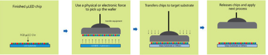
Source: CTimes
During the production of µLED, millions or even tens of millions of micron-grade LED chips must be accurately and efficiently transferred onto circuit boards. For example, for 8K televisions, as many as 48 million particles must be transferred, and even if 10,000 pieces are transferred at a time, this process needs to be repeated 2,400 times
Dr. Chih-I Wu, Head of ITRI’s Electronic and Optoelectronic System Research Laboratories, also pointed out that even though producing micron-sized µLED chips is not easy, there is equipment that can be used to do it, and the real problem lies in quality of yield and uniformity. For instance, when red LEDs are shrunk down to become micron-grade, there is a problem with silicon materials becoming fragile. Nevertheless, it can still be accomplished, and the only solution remaining is an effective mass transfer solution. Because the equipment needed to carry out mass transfer with good yields and in large amounts is highly technologically challenging, at present companies such as Apple, Samsung, and Sony are all actively engaged in research in hopes of making a breakthrough. Dr. Wu also stated that the principle behind achieving mass transfer is actually very simple. First something must be produced which can accurately absorb µLED chips, and then they must be transferred onto a target back panel and be released with precision. In principle, this can be done using vacuum, static, sticking, UV or electronic effects. The key problem lies achieving a suitable yield and whether the cost varies inversely with production capacity. If production capacity is not a consideration, contemporary mass transfer equipment such as those which employ the “Pick-and-Place” method can be utilized to produce µLED display panels; however, the cost is extremely expensive.
To date there have been a few companies which have announced some success on small-sized boards, such as Taiwan’s PlayNitride, Epistar, and LuxVue (which was purchased by Apple), Japan’s Sony, and Samsung. Furthermore, Taiwan’s AU Optronics Corporation has developed the world’s highest resolution 8” µLED display. Nevertheless, these companies used mass transfer technologies in constructing the display.
Compared to μLED, which urgently requires huge transfer technology for a solution to its mass production issues, Mini LED, which has 50-60 micrometer chips, has the capacity to be produced entirely using existing manufacturing equipment. As a result, LED manufacturers are currently choosing to use it as a transitional product, and even Samsung and Sony, which have launched Micro LED products in the past, may manufacture Mini LED products, which can be produced using existing equipment. ITRI began research and development of µLED technologies in 2009; however, it was just a start and they did not move in the direction of mainstream display applications. Nevertheless, as the market and technology has progressed, they have gradually become aware of its market potential. “At the time we believed that it was possible with OLED, and we were certain that it could be done with LED,” said Dr. Chih-I Wu. He pointed out that in theory LED could replace all of the OLED products of today, and the only problem is manufacturing costs and what is known as C/P value. If the prices of the products that we produce are excessively high, then interest will be lacking, and there will be no development value.
As for mass transfer technology, Dr. Chih-I Wu confided that ITRI already has some related solutions now; however, he is not able to elaborate on the situation and only replied that this year there will be some related technological publications and urged everyone to wait and see. However, he also believes that currently the most feasible manufacturing processes for mass transfer are ones using 6-inch-8-inch wafers, which are primarily for small-sized display screen applications. He believes that large display applications can only be made by putting smaller pieces together to solve manufacturing cost problems. As for the forms of technology, he thinks that transfers will be made with adsorption transfer methods, Van Der Waals, or other forces. Due to the difficulty of developing mass transfer technologies and constraints on mass production and yields, the µLED application markets will have an “M-shaped” development, meaning that they will first began from very large and very small dimensions before finally being gradually developed for the largest-sized consumer electronics and televisions. However, whether or not they can be developed for mainstream consumer product markets and even replace the current OLED televisions and LCD televisions of today will depend on the cost of production at the time. Dr. Chih-I Wu stated that because LED’s are characterized by having smaller light emitting areas than the size of devices, they are extremely well-suited to being placed together to produce extremely large display surfaces, and this is particularly the case with large-sized display screens in outdoor or public areas. In addition, these applications have sensitive cost considerations and will therefore be the first commercial markets for µLED screens. After they are utilized on large-sized screens, they will be used in applications with extremely small-sized screens, such as wearable devices and AR/VR devices – especially in AR/VR devices. Dr. Chih-I Wu went on to explain that µLED characteristics, such as its brightness, low power consumption, and high response speed make it extremely well suited for use in these applications. Hence, it can not only overcome problems associated with displays during daylight, but also improve power consumption while simultaneously satisfying the high-speed display requirements of computer games. Dr. Chih-I Wu believes that µLED will enter into consumer markets and be especially common in regular home electronics markets. He believes that currently the manufacturing costs of µLED are extremely high, and even if the manufacturing processes mature, the costs will still be higher than those for LCD or OLED screens. Similarly, even if the display performance is excellent, it will still be difficult to persuade consumers to buy them. Therefore, we will still have to take some time to observe their development.
Rumors about the next Apple Watch, Series 4 have been spread before the official announcement. Apple has unveiled its project with TSMC to develop applications using silicon wafers to solve the issue of mass transfer last year and the market has expected that Apple will adopt its own Micro LED display on the new Apple Watch since then. It was anticipated that Micro LED display might be adopted in the new Apple Watch but as indicated above OLEDs will still be used.