Vertical Divider
Sony Explains Crystal TV’s μLED Technology -- 20μm LEDs and Micro IC Drivers
Back in 2015, the CEO of a small μLED start-up[1] participated in a DOE forum and boldly predicted that by 2020, his company would produce a commercially viable 65” TV. It didn’t happen, but that company remains and is a leader in the erstwhile industry. In 2020, the first commercial μLED TV was announced by Sony, but it was much larger than 65” and targeted a niche market, between giant LED displays for stadiums and signage and the 200m consumer TV market. Recent estimates put the size of the market in 2021 at 100 sets, supplied by Sony and Samsung.
The suppliers faced a number of challenges:
Samsung and Sony were able to solve most of the issues associated with μLED TVs, except, of course, the ultimate goal of producing a 65” TV for <$4,000. They adopted, what are today called Mini LEDs 20 to 50 μm; more costly than a 10 μm LED but more efficient. The used PCBs instead of glass for the backplane and configured a process of connecting multiple PCBs to tile virtually any size large TV. To minimize the color shift and to variable on times, they placed driver logic under each sub-pixel. They designed the edges of the connectable PCBs to make the tile connections invisible. They used a Pick-and-Place transport process to move the LEDs from the wafer to the display substrate. These systems are expensive and slow, but they work. The companies have found a solution to the LEDS catastrophic failures over time, apparently with some form of redundancy.
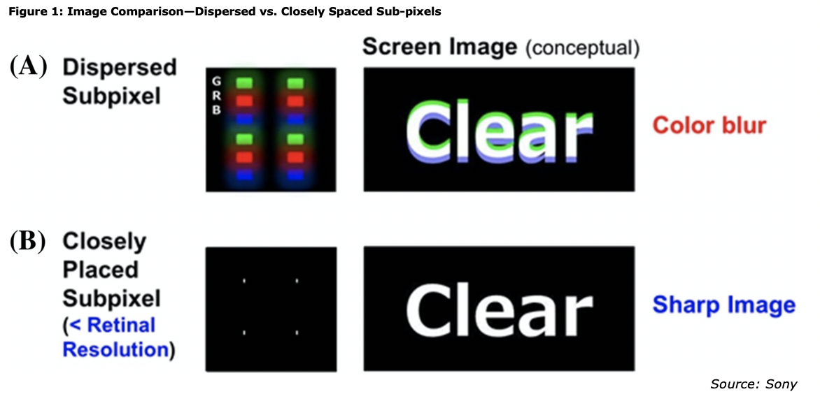
Sony recently released details of its Crystal LED display in the Journal of the SID. The latest Crystal display uses 20 μm LEDs, which Sony claims was key to achieving RGB subpixels with 80 μm pitch. Sony points to wider pitches that cause the eye to see distinct color lines - similar to the 'chromatic aberration/fringing' in lower quality camera lenses. Color fringing is one factor that will affect display realism Given the display size, the wider the pitch the poorer the off-axis performance. To solve that problem, Sony ensured that the emissions from the LED are basically Lambertian and do not produce an off-axis color shift. Perhaps, the comment was a dig at Samsung Visual’s The Wall, which uses μLEDs twice as large.
[1] Charles Li, PlayNitride
Back in 2015, the CEO of a small μLED start-up[1] participated in a DOE forum and boldly predicted that by 2020, his company would produce a commercially viable 65” TV. It didn’t happen, but that company remains and is a leader in the erstwhile industry. In 2020, the first commercial μLED TV was announced by Sony, but it was much larger than 65” and targeted a niche market, between giant LED displays for stadiums and signage and the 200m consumer TV market. Recent estimates put the size of the market in 2021 at 100 sets, supplied by Sony and Samsung.
The suppliers faced a number of challenges:
- Modern TVs require millions of sub-pixels, and the cost varies exponentially with the LED size, while the efficiency has an inverse relationship with size.
- As with all μLEDs, blue and green use INGaN and have dissimilar efficiencies. Red uses AlGaInP and is also less efficient than blue.
- Systems that transport μLEDs from a wafer to a display substrate are inherently immature and while promising, have not been qualified for commercial production
- As the length of the display electrodes increase, the RC constant loss causes slight deviations in the update velocity for a given display row.
- The target TV size not prepared for 200”+ substrates
- The ultimate size of the μLED TV makes it difficult to transport.
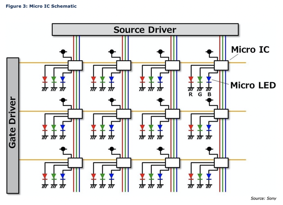
Samsung and Sony were able to solve most of the issues associated with μLED TVs, except, of course, the ultimate goal of producing a 65” TV for <$4,000. They adopted, what are today called Mini LEDs 20 to 50 μm; more costly than a 10 μm LED but more efficient. The used PCBs instead of glass for the backplane and configured a process of connecting multiple PCBs to tile virtually any size large TV. To minimize the color shift and to variable on times, they placed driver logic under each sub-pixel. They designed the edges of the connectable PCBs to make the tile connections invisible. They used a Pick-and-Place transport process to move the LEDs from the wafer to the display substrate. These systems are expensive and slow, but they work. The companies have found a solution to the LEDS catastrophic failures over time, apparently with some form of redundancy.
Sony recently released details of its Crystal LED display in the Journal of the SID. The latest Crystal display uses 20 μm LEDs, which Sony claims was key to achieving RGB subpixels with 80 μm pitch. Sony points to wider pitches that cause the eye to see distinct color lines - similar to the 'chromatic aberration/fringing' in lower quality camera lenses. Color fringing is one factor that will affect display realism Given the display size, the wider the pitch the poorer the off-axis performance. To solve that problem, Sony ensured that the emissions from the LED are basically Lambertian and do not produce an off-axis color shift. Perhaps, the comment was a dig at Samsung Visual’s The Wall, which uses μLEDs twice as large.
[1] Charles Li, PlayNitride
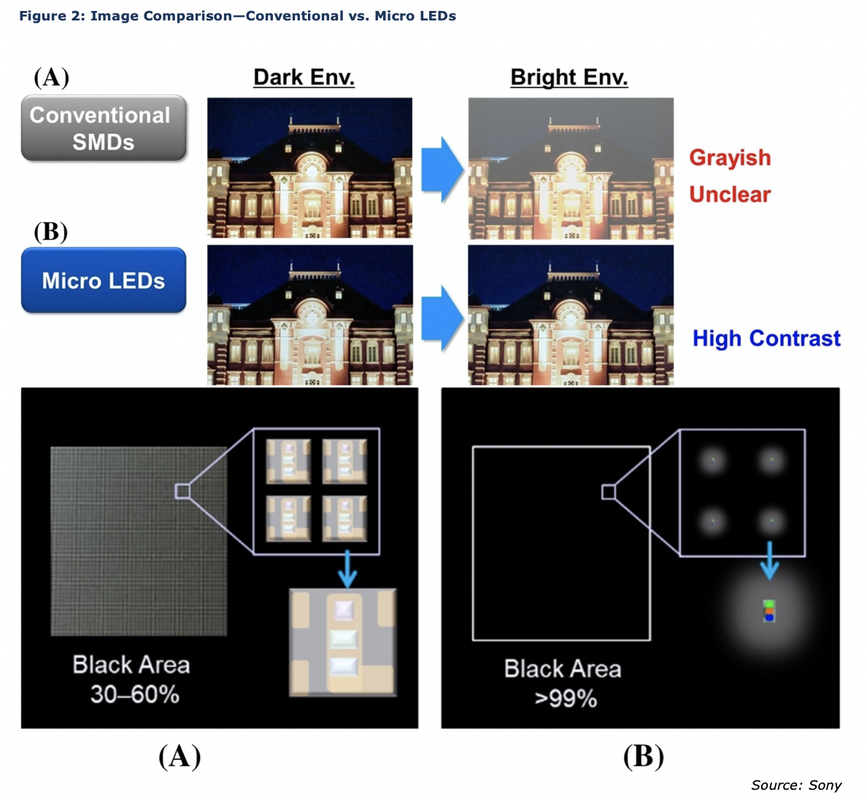
The surface of the LED is just 0.003 mm², and the pixel pitch is 1.2mm pitch, resulting in non-LED surface of over 99%, resulting in a device that’s almost perfectly transparent. The typical 'SMD' LED display has a black area of 30%-60%, typically. Sony measured the scattering effect of traditional LEDs and found that the scattering reflectivity of the non-black areas was as high as 80 times the level of the black areas and that really affects the contrast ratio when the display is in normal ambient lighting. Sony reached its design by using the data it collected to calculate the amount of black needed to give 10,000:1 contrast in ambient light of 100 lux and with display luminance at 1000 cd/m².
Sony uses pulse width modulation (PWM) driving by micro ICs in the active matrix system for each sub-pixel, which has lower drive current than an external driver improving both the constant luminance and color performance. The active matrix scheme according to Sony has no delays in illumination due to the RC constant and eliminates rolling artefacts with black frame insertion.
Sony encapsulated all the LEDs with special resins that resist deterioration despite the high level of photons in a small area. Small LEDs within the pixel provides a seamless look in a tiled display that is assembled from modules.
Sony said that the distortion from the self-weight of the modules when stacked is from thermal expansion. Sony said that the green and blue μLEDs in the display were co-developed with Nichia Corp but didn't specify the source of the red μLEDs.
The companies demonstrated the ability to innovate and some of the results are transferable to products. Variable size TVs could be designed to match the target space, the driver on a sub-pixel is useful in any size TV and could reduce the DDIC costs and make the product fewer dependent semiconductors and cyclical shortages. The companies are qualifying new transport systems – Samsung is attempting to use IJP for its nano LED process. Independent of the μLED TV makers, GaN μLEDs are being produced on a single wafer with equally high efficiencies. While μLEDs have yet to achieve CE product level capability, they are making progress.
This commentary was adopted from an article in Display Daily written by Bob Raikes <[email protected]>
|
Contact Us
|
Barry Young
|


