Vertical Divider
|
Samsung to Ship 43m Galaxy S9 Series Smartphones in 2018
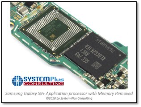
March 19, 2018 Samsung Electronics has prepared two million more Galaxy S9 series devices than the previous Galaxy S8 products for the first-year sale in 2018 as the firm expects to achieve a greater Y/Y sales through aggressive marketing, according to a Korea-based The Bell report. After taking yield rates into account, Samsung should ship 43 million Galaxy S9 devices in 2018, with quarterly shipments in sequential order reaching 12, 13, 10 and 8 million units, respectively, said the report. Samsung shipped about 41 million Galaxy S8 phones in 2017 compared to 48 million units of the Galaxy S7 in 2016. Samsung previously launched a series of "buy one get one free" campaigns to promote its Galaxy S7 in North America and could use a similar low-price tactics for the Galaxy S9 this time, as the company is willing to sacrifice 5-10% of operating margin in exchange of replacement demand for its new models, said the report. Looking at a teardown of the Galaxy S9, Samsung used mSAP (modified semi-additive processes) in the design and construction of its application processor. Figure 1: Samsung Exynos 9810 Chipset (Memory removed) Source: System Plus Consulting
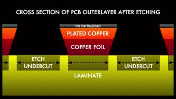
This manufacturing technique is similar to Apple’s in its iPhone X PCB design, and represents the next step in advanced semiconductor packaging. By using this technique, a producer is able to build a semiconductor device by adding material, rather than by etching away material, which is typically the case. To illustrate, the next figure shows a typical etch copper trace (side view) after etching, and it can be seen that the shape of the copper trace is not a column, but a trapezoid. Such a misshaping can cause impedance issues in circuits that while not a big problem with lower frequencies begin to have an increasing effect in 4G and an even bigger one for 5G. Figure 2: Etched PCB Trace Shape Source: Printed Circuit Board Fabrication.com
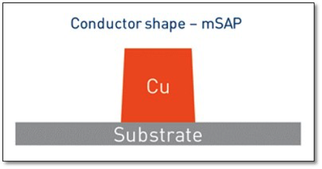
The mSAP process, shown next adds copper traces layer by layer; similar to the way an additive manufacturing tool builds up a prototype one layer at a time, which creates far more precise traces that have fewer problems as communication frequencies increase. While Apple championed the process improvement, with Samsung joining the movement, large-scale PCB manufacturers will have little choice but to adopt the necessary tools and process changes that make this technology work. Figure 3: mSAP TRACE SHAPE Source: Electronic Design
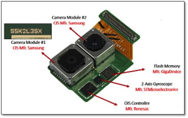
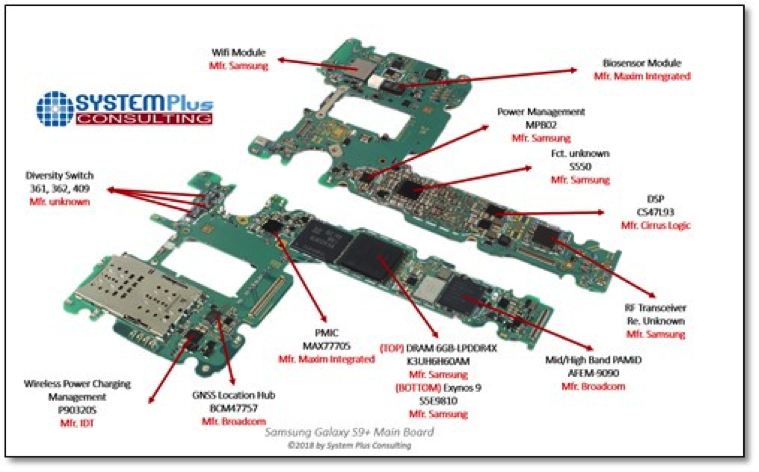
Going further, according to System Plus Consulting, who did the teardown we illustrate here, ST Micro is a big beneficiary of new features in the S9, as their inertial measurement module was added in addition to the STM sensors already used previously, and STM’s gyroscope module also resides in the S9 camera module, which adds stability functions to the camera. While the S9 does not have the ‘true-depth’ camera used by Apple for face recognition, the device can recognize fingerprints, iris, or facial biometrics for identification and the camera module has the ability to automatically adjust the aperture according to the amount of light being sensed, which allows for better pictures in low-light settings without any adjustments by the user. Further, the S9 uses a Broadcom RF module, which contains power amplifiers, BAW filters, antenna switches, and a variety of other mid to high band circuitry encapsulated in one device, similar to one used in the iPhone X. By incorporating these circuits in one package, performance is improved (shorter connections, etc.) along with space and reliability, and such modules will increasingly be built using mSAP and other advanced semiconductor packaging techniques that will allow such devices to maintain thin form factors while improving functionality. While the consumer would certainly be unaware of what goes on under the hood of the S9 and the iPhone X, and neither seems to have attracted an increasingly blasé consumer, these two devices have incorporated a number of new technologies that push the edges of the smartphone supply chain, and advance the industry to a new inflection point that will help to change the shape of mobile devices. Whether these changes will excite consumers remains to be seen, and many will be invisible, but they will make possible the further evolution of the mobile device space, which will have an impact on both the supply chain, and the way in which mobile devices will be used in the future. Figure 4&5: S9 Main Board (top) and Dual camera module - Source: System Plus Consulting (Bottom) Source: System Plus Consulting
|
|
|
Contact Us
|
Barry Young
|

