Vertical Divider
Musing on Competitive Technology
Samsung Experiments w/Blue Nanorods as an Alternative for Blue OLED Material
March 15, 2020
We recently reported that Samsung Display was concerned that their QD-OLED plan was in jeopardy, because it relied on blue fluorescent material for the light source and had developed a back-up plan to replace the blue OLEDs with nano LEDs that were Ink Jet Printed unto the substrate. The QD Display 1.0 program is how SDC refers to the use of blue OLEDs and QD 2.0 is the use of GaN based blue light emitting nanorods. Samsung wants to decide in the second half of the year whether they will go with this QD Display 2.0 instead of 1.0 for the 2nd and 3rd phase investment of a total 11 billion dollar project. So far, 2 billion dollars was executed as the 1st phase to produce 30K substrates/mo. Ink jet printing the nanorods onto the substrate encompasses lifting the nanorods off their Si substrate, putting them in a solvent and then printing them onto the display. This process requires that the nanorods self-align using some sort of electrostatic process currently, the self-alignment rate (two edges of the nanorods must seat on cathodes and anodes) is about 70~80%.
DSCC recently described the process, calling it QNED technology in which GaN-based blue light emitting Nanorod LEDs are used as the blue light source. The advantages of the QNED structure over QD-OLED include higher efficiencies and brightness, longer lifetimes and elimination of image sticking. Additionally, since GaN Nanorods would require a less costly encapsulation process.
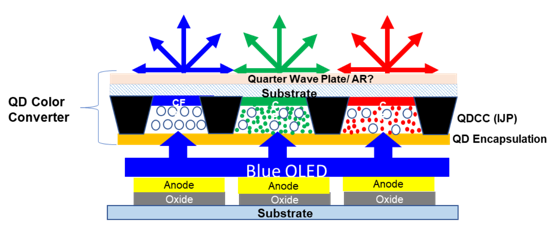
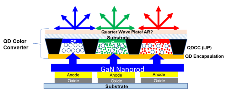
A simplified cross section of the QD-OLED and QNED device is shown below where the OLED is replaced by the GaN Nanorod LED.
Figure 1: Comparison of Panel Structures
Source: DSCC
Blue GaN Nanorod LEDs:
GaN nanorods, essentially free from crystal defects and exhibiting very sharp band-edge luminescence, have been grown by reactive direct-current magnetron sputter epitaxy onto Si (111) substrates at a low working pressure of 5 mTorr. Upon diluting the reactive N2 working gas with a small amount of Ar (0.5 mTorr), we observed an increase in the nanorod aspect ratio from 8 to ~35, a decrease in the average diameter from 74 to 35 nm, and a two-fold increase in nanorod density. With further dilution (Ar = 2.5 mTorr), the aspect ratio decreased to 14, while the diameter increased to 60 nm and the nanorod density increased to a maximum of 2.4 × 109cm−2. Yet, lower N2 partial pressures eventually led to the growth of continuous GaN films. The observed morphological dependence on N2 partial pressure is explained by a change from N-rich to Ga-rich growth conditions, combined with reduced GaN-poisoning of the Ga-target as the N2 gas pressure is reduced. Nanorods grown at 2.5 mTorr N2 partial pressure exhibited a high intensity 4 K photoluminescence neutral donor bound exciton transitions (D0XA) peak at ~3.479 eV with a full-width-at-half-maximum of 1.7 meV. High-resolution transmission electron microscopy corroborated the excellent crystalline quality of the nanorods.
Catalyst-free GaN-NR growth has successfully been demonstrated by chemical vapor deposition (CVD), hydride vapor phase epitaxy (HVPE) physical vapor deposition (PVD) (i.e., molecular beam epitaxy (MBE) and direct-current magnetron sputter epitaxy (DC-MSE) Magnetron sputter deposition is a well-established method which can easily be up-scaled to grow over very large areas for industrial applications. In addition, it provides for low-energy ion assisted deposition which can be used to lower the growth temperature. DC-MSE is a promising method as it employs ultra-high vacuum (UHV) conditions and ultra-high-purity source materials, thus combining the advantages of magnetron sputter deposition and those of MBE. DC-MSE has also been demonstrated for the growth of high quality GaN continuous epilayers as well as NRs. Besides the mass and energy of incident reactive species, selective control of metal–ion fluxes, substrate bias synchronized to probe gas–ion or metal–ion irradiation, is available in a more controlled manner with more complicated sputtering configurations being employed, such as high-power impulse magnetron sputtering (HiPIMS), hybrid HiPMS/DC-MSE co-sputtering using synchronized pulsed substrate bias, MSE with applying external magnetic field, etc. These methods have been applied to achieve single-phase multi-nary alloys grown at low temperature, which demonstrates a high capability to use MSE for the material growth of high-performance optoelectronics.
DC-MSE of GaN-NRs/Si (111) has been reported, using a pure N2 environment, with a total pressure varying from 5 to 20 mTorr. The NRs exhibited excellent optical properties with band-edge (BE) emission at 3.477 eV with a full-width-at-half-maximum (FWHM) value of 1.7 meV when grown at the highest N2 partial pressure value of 20 mTorr. This coincided with the best achieved structural quality, highest aspect ratio, and highest growth rate of the NRs.
However, working at high pressures of pure N2 with DC-MSE, such as 20 mTorr, poses several challenges. For example, it is difficult to maintain a stable process at such pressures when sputtering in a N2-rich environment. Sputtering a metallic Ga target under such conditions results in the formation of a GaN compound of low electrical conductivity on the surface, so called target poisoning, which is a major issue. Target poisoning is known to strongly limit the achievable deposition rate and, in some cases, inhibit sputtering altogether. Moreover, after the growth of GaN-NRs using a pure nitrogen environment, target poisoning effects make it impossible to grow continuous GaN epilayers, which require an Ar/N2 mixture, using the same nitride target. Another disadvantage of using high working pressures, like 15 or 20 mTorr, is that throttling of the UHV pumping system often is required in order to maintain a stable pressure. Such practice reduces the pumping speed and thus, effectively eliminates the UHV conditions during growth, which increases the probability of impurity incorporation into the growing material. A high process pressure also leads to gas scattering of the sputtered Ga which, in turn, leads to a lower degree of utilization of the source material and unwanted deposition of Ga remote from the substrate. It is thus desirable to lower the total pressure and reduce the amount of N2 in the sputtering gas for DC-MSE GaN-NRs growth.
Figure 2: SEM micrographs showing side views (left) and top views (right) from GaN nanorod samples grown at (a,b) PN2 = 5 mTorr; (c,d) PN2 = 4.5 mTorr; (e,f) PN2 = 3.5 mTorr; (g,h) PN2 = 2.5 mTorr; (i,j) PN2 = 1 mTorr pressure on Si(111) substrates.
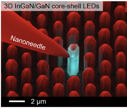
Nanorod structures possess some key features, which potentially are very attractive for use in this application. GaN nanorods with high aspect-ratio and large surface-to-volume ratio can dramatically reduce the dislocation density in the upper part of the nanorods. The light extraction efficiency is expected to increase owing to the non-planar geometry of nanorods. A substantial benefit of the nanostructure is the realization of a core shell structure. Most promisingly, core/shell nanorod structures in which the InGaN/GaN multi-quantum wells (MQWs) grow on the whole cylindrical surface of the nanorods are suggested to be able to effectively increase the active area by a factor of about 4* aspect ratio (as high as 10 X larger emitting surface area) and, as a consequence, increase the total light intensity of the same substrate area. Furthermore, since the dimensions of these structures are small, Nanorods can be blanket coated over the bottom electrode and the TFTs can be used control the pixel switching. In essence, a “self-emissive” blue nanoLED pixel can be made and the resolution of such a display in theory will be limited by only the underlying TFT layer.
Figure 3:Planar LEDs vs. Nanorods
Figure 3:Planar LEDs vs. Nanorods
Source: DSCC
Figure 4: 3D InGaN Core-Shell LED
Source: Appl. Phys. Rev. 6, 041315 (2019)
QNED structure: The QNED structure consists of the following:
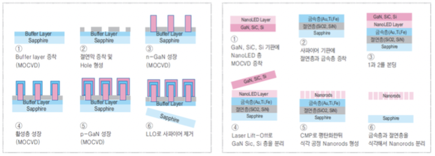
Figure 5: Nanorod Liftoff
- Backplane
- Blue GaN Nanorod LEDs
- Quantum Dot Color Conversion
- Backplane: For TV applications, the backplane will likely be be high mobility IGZO oxide TFTs which is same as the current oxide TFTs used for manufacturing OLED TV panels. Therefore, Samsung’s existing (or to be installed) QD-OLED equipment can be used to manufacture the backplane.
- Blue GaN Nanorod LEDs: This includes two parts a) Nanorod Fabrication b) Nanorod integration with the backplane to form the device.
Figure 5: Nanorod Liftoff
In the top down approach, patterning methods such as etching techniques, are introduced as a low-cost but highly efficient way toward fabrication of high-aspect-ratio 3D GaN micro-/nanostructures. A straightforward method to fabricate GaN nanoLEDs is to etch planar GaN LEDs with nanomasks. The GaN nanorods can be defined by various methods like conventional photolithography, e-beam lithography, and nanoimprint lithography or other low-cost methods, such as SiO2nanosphere lithography as shown below. Dry etching methods, such as RIE-ICP, can be used to achieve high aspect ratio.
The nanorods are said to have a height of 2 um and a diameter of 0.62 um. Exact control of the dimensions over large areas might be a challenge. Further, although the luminous efficiency in theory can be high, it remains to be proven in the fully assembled device. Aggregation effects, size, shape and strain variation in these nanorods can impact the efficiency, color or both.
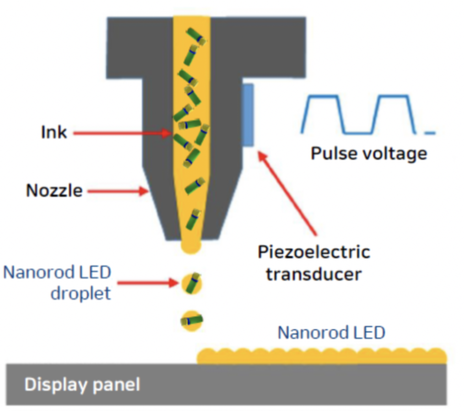
b) Nanorods integration: The nanorods are then integrated onto the backplane to form the device. Inkjet printing technique is currently selected as the means of deposition of the Nanorods. Since the dimensions of the Nanorods are small and this could result in random orientation of the nanorods, first, an electrode is formed on the TFT, for the purpose of alignment with an electric field. The exact process is still not well understood but the sequence of the steps for the integration is as listed below:
Figure 6: Nanorod Integration
Source: KTB Securities and Samsung Patent
I. First electrode formation on the TFT and insulation layer deposition: Achieved by depositing ITO, Al, Ti, Au, etc. by PVD and patterning by wet etch. An insulation layer is subsequently deposited over the first layer. The insulation layer maybe a SiNXor SiO2 material deposited by CVD or ALD equipment.
II. Inkjet Printing of Nanorods: The nanorods dispersed in a solvent are then inkjet-printed onto the described layer. Currently, we expect this to be a blanket coating on the substrate since pixel level color definition is not required for the blue nanorods. Potential challenges with inkjet methods include clogging of printheads due to micron sized dimensions of the Nanorods, poor dispersion of the nanorods in the solvent of choice, inkjet stability and uniform drying of the solvent over large area glass sheets etc. Having a larger diameter nozzle may help some of these problems, but it remains a challenge.
Figure 7: Nanorod Printing
Source: DSCC
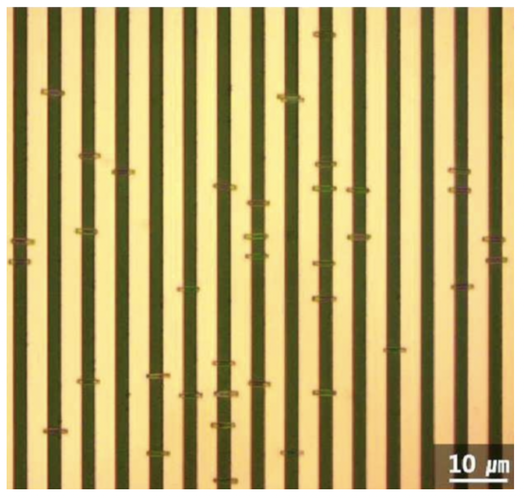
III. Nanorods Alignment: Nanorods are then aligned by applying a voltage to the first electrode. It is still unknown as to how this would be achieved and how efficient the alignment process is and if good contacts can be achieved by this process. A Samsung patent showing an aligned Nanorod is shown below.
Figure 8: Nanorod Alignment
Figure 8: Nanorod Alignment
Source: Samsung Patent- WIPO: KR1020190137742
IV) Formation of second electrode for driving nanorods: The second electrode is then deposited by PVD on nanorods. The materials used for this layer is likely selected from Ti / Au or ITO. This is subsequently followed by selective etching to define the aperture.
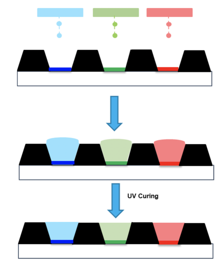
3) Quantum Dot Color Conversion: Since GaN Nanorods emit blue light, we believe there will be no change in color conversion methodology when compared to QD-OLED. The quantum dots will absorb the blue light and down convert it to red or green in the red and green pixels respectively. An additional RGB secondary filter is likely to be used to prevent unintentional excitation of QDs as well to prevent blue leakage due to in-sufficient blue light absorption by Cd-free QDs. The QDCC is expected to be formed by inkjet printing of QDs dispersed along with scattering particles a in solvent free monomer system. The blue pixel will be coated with only scattering particles. A schematic of the process flow is shown below:
Figure 9: IJP QDs
Source: DSCC
QNED Timeline and Cost:
Samsung is in the R&D stage now with a target of moving to pilot production in the first half of 2021. If the technology is successful in the pilot line, it is possible that plans for expanding QD 1.0, which will be operational in Q121 would be replaced by QD 2.0. Beyond large area panels QD 2.0 could be used with photolithography of QDCC as an option for high resolution requirements of small and medium sized displays displaying the FMM process used with OLEDs. An LTPS backplane would also likely be required.
The cost of QD 2.0 is expected to be lower than QD-OLED due to the removal of the OLED deposition that would be replaced by IJP equipment. The high cost OLED TFE would also be replaced with a lower cost substitute. However, some or most of these costs would be offset by the numerous process steps involved in fabricating. integrating and printing the Nanorods.
|
Contact Us
|
Barry Young
|

