Vertical Divider
Rush to Produce GaN RGB nano-LEDs on a Single Wafer
A UK start-up, Porotech, is preparing to o commercialize porous GaN, opening the door to high performance optoelectronic devices with unexpected properties, reports Rebecca Pool. A relatively unknown material from a newly minted UK start-up is set to makes waves in the rapidly growing GaN market. The 'porous GaN' is attracting interest in compound semiconductor circles. And thanks to £1.5 million in investment funds, University of Cambridge spin-off, Poro Technologies - or Porotech - is on track to be one of the first companies to bring this mesoporous version of GaN to market
Porous GaN can be regarded as a semiconductor composite of solid GaN and air. Professor Rachel Oliver, Co-founder, and Chief Scientific Officer of Porotech, and Director of the Cambridge Centre for Gallium Nitride said: “Porous GaN is basically GaN with holes in it that are a few tens of nanometers across.” “With porous GaN we can engineer a wide range of material properties... and offer a new material platform to build semiconductor devices on,” she adds.
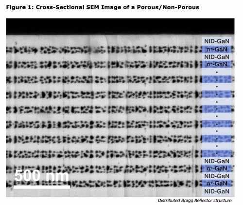
The Porotech team creates the nanoscale porosity in GaN wafers using electrochemical etching. The etch is conductivity selective and responds differently to the material depending on its doping density. Porosity is created in doped layers while undoped layers are left undamaged, allowing complex 3D nanostructures to be created. According to Oliver, the etchant flows to and from the doped layers via the many nanometer-scale channel-like defects - dislocations - that exist within any GaN wafer. “Even your best quality GaN wafer will still have around 105 dislocations per square centimeter,” she explains. “So the etchant will flow down a dislocation and when it hits the doped layer will etch it very quickly to create the porosity before continuing down that channel to the next doped layer.” “We can take an entire wafer and using this conductivity selective etching mechanism to create GaN [structures] with a whole new set of properties that haven't been available before,” she adds. “It's very cool from a commercial perspective.”
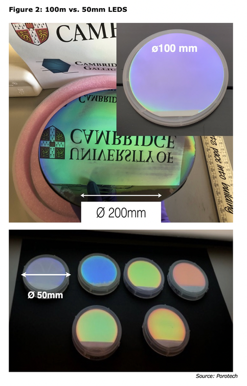
Oliver and Porotech chief executive, and co-founder, Dr Tongtong Zhu, claims the method has been tried and tested with wafers up to eight inches in diameter and it will seamlessly scale to even larger wafer sizes. Oliver, Zhu and colleagues have fabricated several components and device prototypes. They have demonstrated highly reflective Distributed Bragg Reflectors (DBRs) - or 'Poro Mirrors' - based on wafers comprising alternating layers of solid and nanoporous GaN. InGaN LEDs were then grown on these epi-ready DBR pseudo-substrates that were some 25% more energy efficient than standard LEDs. “This DBR substrate is fully compatible with GaN so a customer doesn't need to process anything differently during LED fabrication but can still get a brighter and more efficient LED,” points out Zhu.
Porotech has also joined forces with other institutions and start-ups to fabricate thermal sensors that used porous GaN layers as on-chip thermal insulation. And in a novel technology twist, the team has filled the pores in a porous GaN wafer with a halide perovskite to create an optoelectronic material with longer-lasting luminescence. “These luminescent perovskites are useful in solar cells and LEDs but degrade very quickly,” says Oliver. “We can slow this degradation down with porous GaN.” The Porotech pilot plant was built at Cambridge by transferring production process from the laboratory to the plant. The company is also working with foundry services, wafer producers and integrated device manufacturers, and hopes to license out technology in the coming years. “We've been working to get the company off the ground for several years and we aren't going to stop now,” says Oliver. “There has been no other time when GaN is rising so quickly, and we have to keep up our momentum.”
|
Contact Us
|
Barry Young
|


