|
OLEDON Develops Deposition Methodology to Reach 2000 dpi for OLED Displays
July 10, 2017 Three years have passed since the first QHD (about 515 ppi) OLED was used in the Galaxy Note4 in 2014, but OLED resolution is still in QHD. In order to manufacture high-resolution OLED > UHD, FMM of less than 15 μm is required, but has not yet been used in mass production. Professor Hwang Chang-Hoon, CEO of OLEDON, a venture business of Dankook University, proposed that the planar source FMM deposition technology is the only solution for a high-resolution OLED manufacturing process over UHD a recent Seminar held on June 30 at Yeouido FKI Conference Center. Professor Hwang Chang-Hoon said, “To improve the resolution of AMOLED, the angle of flight of organic molecules should be reduced to less than 10 degrees and the aspect ratio of TFT devices should be maintained at 1.0 level. The evaporation angle (incidence angle) of the currently known linear source is about 40 degrees, and the shadow distance is about 3 um. Therefore, the ratio of the pattern width, the shadow distance, and the aspect ratio can be increased at the SUHD level AMOLED patterning process. Ultimately, the current patterning technology loses the flatness of the film.” In addition, Professor Hwang Chang-Hoon said, “Linear deposition technology has limitations in achieving resolution higher than QHD, and development of planar source FMM deposition technology is the only way to manufacture OLED with 2000 ppi or higher.” Figure 1: Limitation of Linear Source to Achieve High Pixel Density 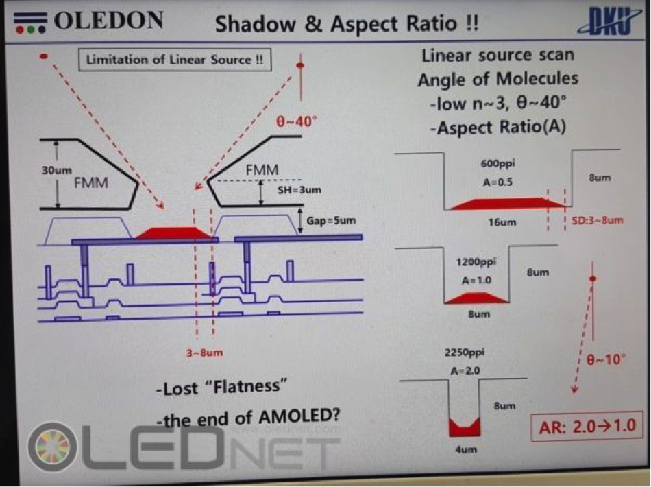
Source: OLEDNET
The shadow distance measured by OLEDON’s planar source FMM deposition technique ranges from 0.68 to 1.05 μm and the angle of incidence is 13 to 19 degrees and converting this result to resolution makes it possible to fabricate a device with a maximum of 1500 ppi. On the other hand, with the newly developed Xplane source, the shadow distance was 0.38 ~ 0.56um and the incident angle was 7.2 ~ 8.0 degrees, it is possible to manufacture up to 3300 ppi device by converting it to the resolution. In the last SID2017, Prof. Jin Byung-Doo and Prof. Hwang Chang-Hoon introduced the world’s first measurement of sub-micron-scale shadow distance using plane source patterning technology, it has been announced that it is possible to manufacture a micro AMOLED device having a Super Ultra (SUHD) resolution of 11K (2250 ppi) or more if scale-up development is applied to large-area OLED display production industry in the future. (Paper title: Planar source evaporation techniques for Super ultra high resolution flexible AMOLED) Figure 2: OLEDON’s Planar Source Achieving High Pixel Density 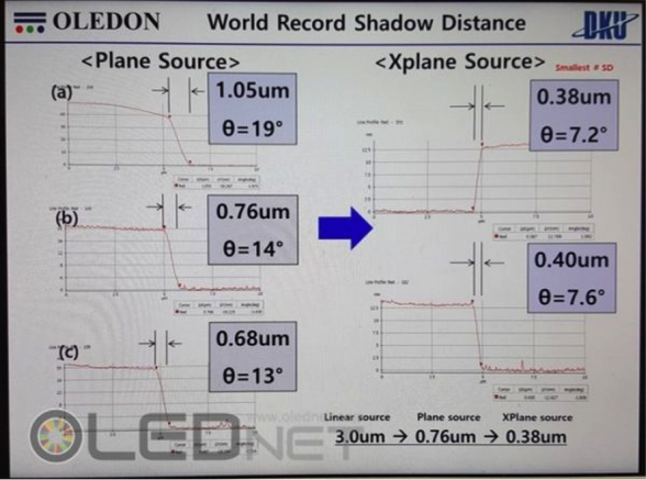
Source: OLEDNET
OLEDON announced that it plans to develop and install planar source FMM evaporator for research, which can manufacture ultra-high resolution micro OLED devices using plane source deposition technology, in Dankook University. (Refer to: OLEDON homepage www.oledon.co.kr) |
Vertical Divider
|
Search by typing & pressing enter