Vertical Divider
Nano-Structured Anti-Reflective Surfaces Reduce Reflections and Decrease Laser Induced Damage Threshold (LIDR)
May 04, 2020
Anti-reflective (AR) thin film coatings are critical in optical applications where light throughput must be maximized, or in situations when back-reflections would be detrimental. Traditional AR coatings are made of one or more layers of dielectric material deposited on the surface of optical components. These layers are designed to reduce reflections across a specific wavelength band through destructive interference of the transmitted and reflected light. However, the anti-reflection performance of thin-film coatings is highly sensitive to wavelength and angle of incidence. The coatings also typically decrease the laser induced damage threshold (LIDT) of the optic because of the potential for coating defects across multiple layer interfaces. The high laser intensities used in applications such as materials processing increase the risk of laser-induced damage and lead to component failures.
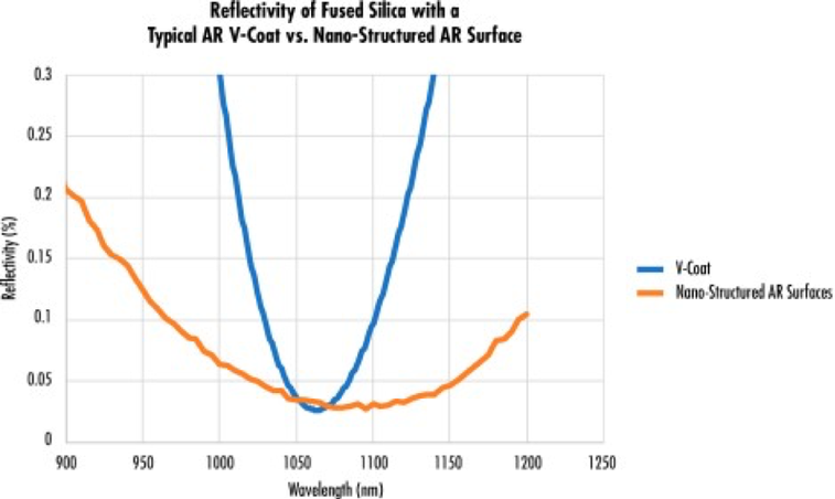
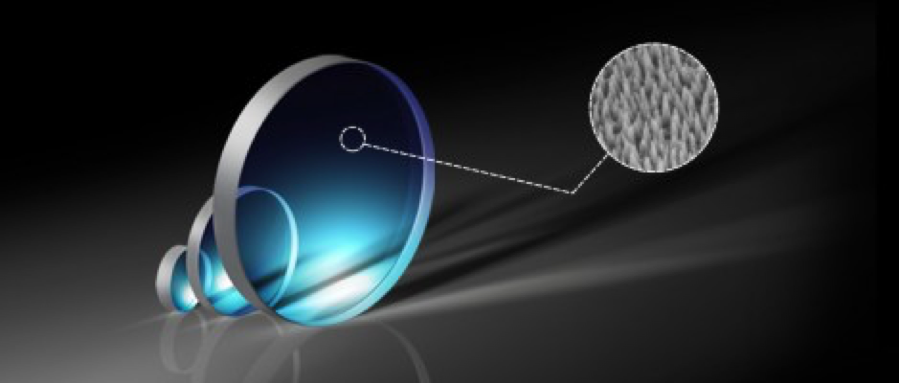
Nano-structured anti-reflective surfaces are an alternative to thin-film AR coatings. They use subwavelength surface structures to reduce reflections while also providing a comparatively high LIDT. Whenever light passes through an abrupt change in refractive index, a reflection occurs according to the laws of Fresnel Reflection. Rather than adding additional material to the optical surfaces, material is removed in such a way as to present a gradually-changing refractive index from air (or other immersion material) into the substrate material, resulting in high transmission over a broader waveband than that of thin-film coatings (Figure 1). The waveband can easily be customized and shifted to be optimized for a specific wavelength region by changing the width, depth, and shape of the nanostructures. One method for producing these nano-structures is reactive ion etching, a “dry” etching process that selectively removes material by a chemical process in a plasma.
Figure 1: Nano-Structured AR Surfaces
Source: Edmund Optics
Additionally, random nano-structured AR surfaces have the potential to be less sensitive to angle of incidence and polarization than standard thin-film AR coatings. For a standard AR coating, a wavelength shift can be seen as the angle of incidence either increases or decreases from the design angle, typically 0 or 45 degrees. This can limit an optical system where scanning of the laser beam is required, such as changing the incidence angle through a window through the scan and thus the transmitted intensity. It has been shown that nano-structured AR surfaces can produce equal transmission for both polarized and nonpolarized light over an angular range of at least 0 +/- 30 degrees [1]. The LIDT of nano-structured AR surfaces can approach that of the uncoated substrate, which is significantly higher than most traditional coatings. This is particularly advantageous for high-power materials processing applications where high intensity and/or beam scanning are encountered.
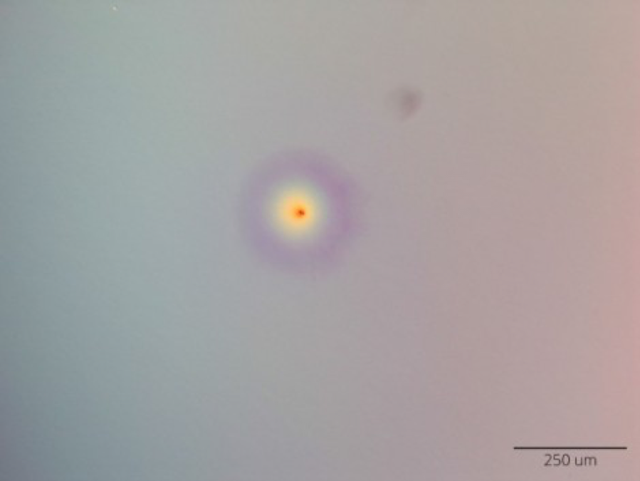
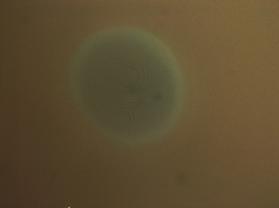
When thin-film coatings experience laser-induced damage, the damage can propagate and cause component failure, degradation of beam quality, and system failure due to back reflections destroying the laser. In nano-structured AR surfaces, on the other hand, laser-induced damage at levels below that of the bulk material threshold typically does not propagate and effectively “melts” the nanostructures back into the bulk material. This slightly increases reflectivity in the localized damage area but does not propagate, which often allows continued use of the optic except in extremely sensitive systems [2].
Figure 2: Typical Propagating Laser-Induced Damage In A Traditional Thin-Film Coating (Top Compared To Typical Laser-Induced Damage In A Nano-Structured AR Surface (Bottom), In Which The Damage Is Difficult To Detect And Approximates The Damage Threshold The Bulk Material. In Both Cases, Damage Was Caused By A 1064nm Laser With A Pulse Duration Of 10ns
Source: Edmund Optics
While these structures have high laser durability, they have low mechanical durability. Abrasion can easily damage the structures, making them difficult to clean and requiring special handing and assembly techniques. However, surface contaminants and abrasion will cause premature damage in any optical coating, and a well-designed system should include provisions to maintain a protected, clean beam line. Additionally, there are many materials processing applications, described below, where this technology can be integrated, and this characteristic is not a detriment.
Integrating nano-structured AR surfaces into materials processing applications
Nano-structured AR surfaces are highly beneficial for debris shields and final focusing optics in materials processing systems. Debris shields are typically disposable components placed between final focusing elements and the surface being treated. They protect sensitive, expensive optical components from contaminants coming off of the processed surface. Because debris shields are typically disposed of and replaced rather than cleaned and reused, they are perfect candidates for nano-structured AR surfaces. With nano-structured AR surfaces the debris shields can now experience higher laser-induced damage, other than that from surface contaminant-driven heating, which in traditional AR coatings can lead to delamination and cascade to catastrophic failure. Additionally, if the debris shield experiences laser-induced damage of the surface structures themselves the damage will no longer propagate, thus extending the debris shield’s lifetime.
Figure 3: Debris Shields With Nano-Structured AR Surfaces Typically Experience Higher Lidts And Less Loss Than Debris Shields Utilizing Traditional Thin-Film AR Coatings While Avoiding The Largest Obstacle Experienced By These Structured Surfaces: The Difficulty Of Cleaning Them
Source: Edmund Optics
The broadband nature of nano-structured AR surfaces can allow for multiple wavelengths to simultaneously experience minimal losses. A growing trend in materials processing is the use of multiple laser wavelengths at once, such as a visible alignment laser and a 1064nm Nd:YAG beam. Additionally, the industry has been seeing the adoption of other wavelengths besides the standard 1064nm. For example, glass cutting often utilizes ultraviolet (UV) lasers to achieve the highest possible precision. The nanostructures can be designed to perform at wavelengths as short as 355nm. Many materials processing applications also utilize ultrafast lasers, which can achieve high peak powers and produce tighter dimensional tolerances than other laser types due to their short pulse durations, from picoseconds down to femtoseconds. These short pulse durations also lead to a broad wavelength spectrum, which increases the difficulty of finding a compatible thin-film AR coating. The broadband nature of nano-structured AR surfaces can provide high transmission across the entire wavelength spectrum of an ultrafast laser, making them a potential solution for short-pulse applications. Nano-structured AR surfaces provide a high-power alternative to thin-film coatings for materials processing and other high-power laser applications. From debris shields to focusing lenses, this technology has the potential to improve laser durability, reduce heat buildup and associated thermal lensing, and increase throughput over a broad range of wavelengths.
Written by By Becca Silver, Optical Engineer, and Cory Boone, Lead Technical Marketing Engineer, Edmund Optics
References
Written by By Becca Silver, Optical Engineer, and Cory Boone, Lead Technical Marketing Engineer, Edmund Optics
References
- C. D. Taylor, L. E. Busse, J. Frantz, J. S. Sanghera, I. D. Aggarwal, and M. K. Poutous, "Angle-of-incidence performance of random anti-reflection structures on curved surfaces," Appl. Opt. 55, 2203-2213 (2016)
- L.E. Busse et al. (2014). Anti-reflective surface structures for spinel ceramics and fused silica windows, lenses and optical fibers. Opt Mater Express, Vol. 4, Issue 12, pp. 2504-2515
|
Contact Us
|
Barry Young
|


