Vertical Divider
Mattrix Technology and the Use of a-Si for OLED Backplanes
We commented on an article in Display Daily regarding Vertical Organic light-emitting transistors (VOLETs). The claim that any a-Si fab could be converted to an OLED fab using this technology seems outrageous. So we took a deeper dive into the technology by speaking with Dr. Max Lemaitre, the founder and CEO and conducing a literature search. Lemaitre comes out of the University of Florida, where original work has been done on Carbon Nanotubes. Since the first demonstration of OLETs in 2003, OLETs have optimizing the single-layer OLET and suppressed the exciton–polaron quenching, however, because of the low dielectric capacitance combined with the intrinsic low mobility, OLETs have needed high working voltages (>100 V) for optimal device performance. .To operate below 10.0 V, the dual-layer dielectric strategy with low-k (defined as the dielectric constant) and high-k dielectrics have been utilized. VOLETs with a single-wall carbon nanotubes have been developed with drain gate voltages of −7.0V and −3.0V.
We commented on an article in Display Daily regarding Vertical Organic light-emitting transistors (VOLETs). The claim that any a-Si fab could be converted to an OLED fab using this technology seems outrageous. So we took a deeper dive into the technology by speaking with Dr. Max Lemaitre, the founder and CEO and conducing a literature search. Lemaitre comes out of the University of Florida, where original work has been done on Carbon Nanotubes. Since the first demonstration of OLETs in 2003, OLETs have optimizing the single-layer OLET and suppressed the exciton–polaron quenching, however, because of the low dielectric capacitance combined with the intrinsic low mobility, OLETs have needed high working voltages (>100 V) for optimal device performance. .To operate below 10.0 V, the dual-layer dielectric strategy with low-k (defined as the dielectric constant) and high-k dielectrics have been utilized. VOLETs with a single-wall carbon nanotubes have been developed with drain gate voltages of −7.0V and −3.0V.
|
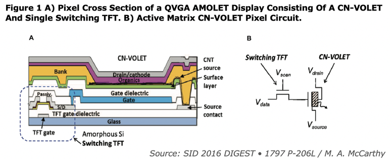
Mattrix optimized the VOLET producing an organic channel with performance comparable to that of poly-Si based TFT driven OLEDs. The device is based on the carbon nanotube enabled vertical organic field effect transistor (CN-VFET). The sub-micron channel length of the CN-VFET allows high currents to be realized at low voltages using organic semiconductors in the channel at low cost. Moreover, OLED layers can be inserted between the channel and drain layers turning the device into a vertical organic light emitting transistor (CN-VOLET) The stacked nature of this new device along with the high optical transmittance of the CNT source electrode (>98% across the visible spectrum) leads to a high aperture ratio in a bottom emission device for the CN-VOLET, which can reduce drive current densities, and in-turn, prolong OLED lifetime. A significant benefit of the CN-VOLET is that it reduces the number of circuit components in the 2T + 1C conventional. A prototype device has been developed by Mattrix using a circuit similar to the figure below.
|
|
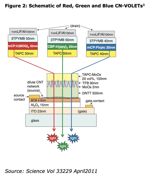
CN-VFET is an OLED stack inserted between the organic semi- conductor of a CN-VFET and its drain electrode with the latter consisting of an electron-injecting, low– work function metal. The CN- VFET substructure controls hole injection into the OLED layers. In the CN-VFET the nano- tubes are spread as a dilute network, well above electrical percolation transmittance spectrum across the gate dielectric sitting on a bottom gate electrode. A metal electrode provides electrical contact along one edge of the network. Because the nano- tubes are used as the source electrode, rather than as the active channel, no separation of metallic from semiconducting nanotubes is necessary. The organic channel layer is deposited as a thin film across the nanotubes and the exposed dielectric, and a metal drain electrode is deposited onto the organic channel layer, completing the device. The trans- conductance originates from a gate field–induced modulation of the Schottky barrier height and width between the nanotubes and the organic channel layer. The OLED layers are inserted between the CN-VFET channel layer, and the drain integrates the driving transistor and the light emitter in the single, stacked device. The CN-VOLET uses a conventional back-channel-passivated amorphous silicon TFT process followed by the CN-VOLET process. The latter consists of three lithographically patterned layers: the gate dielectric layer (a singularly patterned layer stack consisting of silicon nitride, silicon oxide and surface layer), the CNT source layer and the bank layer. The CNT source layer was deposited and patterned by conventional methods. After the bank layer, the organic channel and light emitting layers were thermally evaporated through a shadow mask followed by an aluminum CN-VOLET drain electrode deposited in the same manner. Conventional organic TFTs are generally susceptible to bias stress instability but the stability of the CN-VFET relative to that of conventional TFTs apparently results from the vertical architecture, which limits the time that injected charge spends in the immediate vicinity of the gate dielectric, where traps present a major source for the instability.
CNT films are applied with pulse laser vaporization, using proprietary inks and a JSR slot dye coating tool. The CNT is primarily single wall although there is some bundled double wall CNTs. The benefit is that even with a high duty cycle the driving TFTs do not suffer from heat degradation and the threshold voltage is consistent over time, eliminating the need for compensation circuitry. As a result the drive circuit in a bottom emission OLED display, ala LGD’s TV panels, consists of a single vertical TFT mounted in series with a capacitor resulting in a much larger the aperture ratio than one with complex compensation circuits. Compensation is required for the aging of the OLED, but that can be handled externally.
The DisplayDaily article, which we referenced, proclaimed that the technology would enable a-Si fabs to be easily converted to produce OLEDs and we were skeptical. Looking at the business case:
Greenfield OLED Fabs would use the approach if it proves out. Mattrix has a long way to go as they have produced a small bottom mission panel that was made by JSR, their tool maker and early investor. Samsung Ventures has also made an investment due to work by SIAC. The company is in the process of seeking a second round of funding.
- Existing small/medium a-Si fabs
- An a-Si switching TFT would be too large for today’s high pixel density smartphone displays
- The small/medium OLED market is already saturated with sufficient unfettered capacity to meet the demand for all smartphones for the next 5years.
- Using a bottom emission solution would have negative performance in terms of luminance
- Converting the active matrix from a-Si to IGZO would eliminate the size restrictions of the SW TFT, but nothing else.
- Existing Gen 8.5 a-Si or IGZO LCD fabs
- Would enable the use of these fabs for OLED TV panels to compete with LGD
- Higher aperture ratio would contribute to solving the luminance issue for OLED TVs.
- As more LCD Gen 10.5 fabs are introduced, there are 5 now and could grow to 7 within 2 years, the Gen 8.5 fabs need to be repurposed or TV panel prices will hit rock bottom
- Gen 8.5 OLED fabs for IT and smartphones
- If Gen 8.5 vertical OLED deposition tools work, the Mattrix technology could be combined with IGZO for LTPO using only 9-10 masks instead of 18-20. The benefit is one of cost and capacity, where the fab footprint of an IGZO backplane would not require an expansion or a reduction in capacity
Greenfield OLED Fabs would use the approach if it proves out. Mattrix has a long way to go as they have produced a small bottom mission panel that was made by JSR, their tool maker and early investor. Samsung Ventures has also made an investment due to work by SIAC. The company is in the process of seeking a second round of funding.
|
Contact Us
|
Barry Young
|


