Vertical Divider
|
LTPO Could Replace LTPS for OLED Backplanes
September 03, 2018 IHS Markit predicted that Apple could shift from using LTPS TFT backplanes to usingLTPO (Low Temperature Polycrystalline Oxide)backplanes in future iPhones to conserve battery life.Of course, since Apple doesn’t make displays, they would have to convince, Samsung, LG Display, Sharp, or JDI to develop the technology.IHS believes that LTPO TFT could save between 5-15 percent in power consumption versus LTPS by combine both the technical strengths of c-IGZO and LTPS on a single array backplane. C-IGZO used for the pixel switch TFT have low leakage current and therefore, low power consumption. Experiments have shown good quality of crystal grain size and clear crystallization properties of IGZO using high-resolution transmission electron microscopy (HRTEM) and X-ray diffraction (XRD) patterns. The manufacturing process steps as described by AUO[1]include:
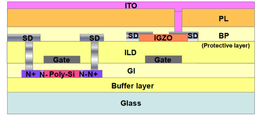
In this AUO experiment, the mobility was relatively low at 5.7 cm2/Vsec, but the point was to demonstrate a working prototype. The process includes the entire excimer laser, ion doping steps for p-Si and PVD for amorphous oxide, so the capex is likely to be more than LTPS. What wasn’t clear from the AUO report was whether they were able to reduce the number of masks or the excimer laser shots required to achieve high uniformity of the grains. IHS’s claim that LTPO would reduce the power consumption by 10%-15% was not verified and the reduction apparently only relates to the power consumed by the backplane. Figure 1: (a) Schematic cross-section of IGZO and LTPS hybrid TFTs with top gate IGZO TFTs (b) Schematic cross-section of IGZO and LTPS hybrid TFTs array technology with bottom gate IGZO TFTs (a) 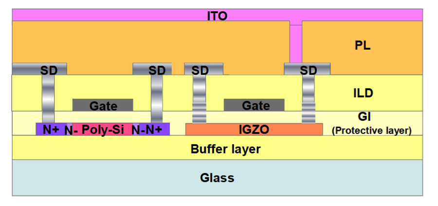
Source: AUO
(b)
Source: AUO
Figure 3: LTPO Power Reduction
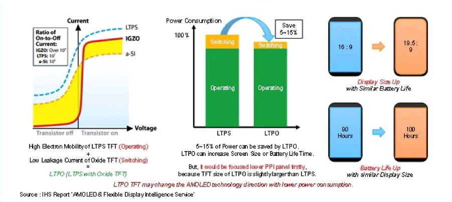
Source: IHS
|
|