Vertical Divider
Improving the Mobility of IGZO
IGZO is a mid-performance semiconductor with typical mobility of 15-20 cm²/Vs in mass production, between a-Si at 0.7 cm²/Vs and LTPS at 50-100 cm²/Vs. Higher mobility leads to smaller TFTs/unit of voltage, which facilitates higher pixel densities and lower power consumption. IGZO also delivers very low leakage current and is relatively stable over time. However, IGZO is a challenging technology where the semiconductor layer needs to be protected by an etch stop layer (ESL) to exclude interaction with the surrounding layers. LG Display (LGD) and Sharp are the only panel makers using the technology, although it is part of Samsung’s QD-OLED and TCL’s OLED IJP programs. IGZO is also being used in LTPO, which was initially rolled out in the Apple Watch Series 5 and will soon be available in Apple and Samsung Smartphones. The graph shows the limits of each active matrix technology related to frame rates and pixel vs. mobility.
Figure 1: Required TFT Mobility vs. Resolution
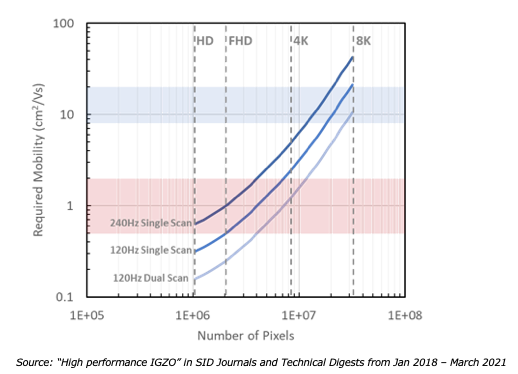
This chart indicates that a 4K display requires a mobility between 1 and 7 cm²/Vs and an 8K resolution between 11 and 50 cm²/Vs. Yet most LCD panels built on Gen 8.5 and smaller fabs use a-Si with a mobility of cm²/V. CSoT on its Gen 10.5 uses IGZO, but BOE uses a-Si as does most other LCD panel makers.
This article presents a review of work done by Amorphyx and is written by Ian Hendy addressing how IGZO mobility can be increased.
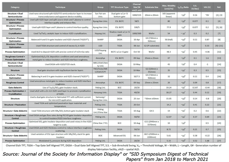
Table 1: Device data for IGZO based TFTs
This article presents a review of work done by Amorphyx and is written by Ian Hendy addressing how IGZO mobility can be increased.
Table 1: Device data for IGZO based TFTs
You can download the table as an XL file here. Research_Table.xlsx
Six approaches to improving mobility have been documented in SID papers based on the data shown in the table above. The first 2 are the most common place ideas from the big display players
Amorphyx is working on using dielectrics/passivation layers and roughness control as two levers as part of their IGZO amorphous metal TFT (AMeTFT) approach. They have shown high mobilities (of 60 cm²/Vs and higher) for a simple ESL type TFT using their smooth amorphous metal gate to influence the surface roughness and aluminum oxide gate dielectric/passivation to improve stability. They are now focusing on further improvements through alternative TFT structures, such as dual gate.
Source: DisplayDaily
Six approaches to improving mobility have been documented in SID papers based on the data shown in the table above. The first 2 are the most common place ideas from the big display players
- Process optimization -- realized by subtly adjusting hydrogen and oxygen flows during depositions or switching to alternate deposition methods
- More complex TFT structures. Dual gate coplanar and top gate self-aligned structures have been used and increase mobility modestly. Split channel TFTs as an approach can make a big difference to mobility but at the cost of larger TFT footprints and have yet to be proven on large area substrates.
- Use an alternative crystallization method, the most common being a thin-film “catalyst” layer, but excimer laser annealing, such as that is used for LTPS, has also been proposed. The downside is increased process cost comparable to LTPS. Approach 4 is to use dual layers of IGZO and related materials in the semiconductor layer. In the early days there was lots of work done on attempts to optimize the constituent weights within the IGZO composition but that now seems to have given way to bilayer constructions, such as IGZO with ITZO. This work is promising, but may or may not lead to additional masks and sputter steps in production
- Change the TFT gate and/or passivation dielectric using a variety of material including silicon nitride/oxide stacks to tantalum or aluminum oxides. The goal is to reduce leakage current for gate dielectrics and improve moisture barrier capability for passivation layers, while avoiding harmful interactions with IGZO. Aluminum oxide ends up being the best option given its low leakage current and low water permeability, plus its ability to play well with IGZO.
- Control the roughness of gate insulator and IGZO interfaces and reduce interface trap states and scattering of carriers in the channel, which is achieved by improving deposition conditions, reducing IGZO thickness or by using amorphous metal gates to enable thinner Al2O3 gate dielectrics and thinner IGZO channels.
What is interesting is that these approaches are broadly additive since they have different mechanisms. Players can try to use process optimization, with a new structure with dual layer semiconductors and at the same time deploy a dielectric/passivation approach and optimize surface roughness. With these, perhaps in combination, we may yet see IGZO TFT reaching the levels of LTPS but without the ELA and doping.
Amorphyx is working on using dielectrics/passivation layers and roughness control as two levers as part of their IGZO amorphous metal TFT (AMeTFT) approach. They have shown high mobilities (of 60 cm²/Vs and higher) for a simple ESL type TFT using their smooth amorphous metal gate to influence the surface roughness and aluminum oxide gate dielectric/passivation to improve stability. They are now focusing on further improvements through alternative TFT structures, such as dual gate.
Source: DisplayDaily