Vertical Divider
Imec Develops Photolithography to Pattern Organic Semiconductors and The Cathode in an OLED-Display Stack
At the International Display Workshop (IDW) 2020, imec, presented a photolithography method for patterning organic semiconductors and the cathode in an OLED-display stack as a replacement for FMM, which is the dominant manufacturing method of patterning the light-emitting-layer (EML) in smartphone size to notebook size panels.
The use of photolithography processes allows for higher design freedom and shows promising results in terms of reliability. For example, imec is capable of creating patterns on top of organic semiconductors with 1µm pitch (line and space), which corresponds to resolutions around 120,00ppi. Also, the transparency of the OLED front plane at higher wavelengths increased from 20% to 70% after cathode patterning. In addition, imec claims no degradation of lifetime. By using photolithography.
The main challenge was the sensitivity of OLED materials to water, oxygen and the photoresist used in a photolithography process Tung Huei Ke, R&D project leader for sensor technology, at imec, said : “Photolithographic patterning of OLED was extremely challenging because of the chemical incompatibility of the photolithography chemistry to the OLED materials. As the first OLED subpixel needs to be patterned at least three times to realize full-color AMOLED array, it was assumed the degradation after multiple photolithographic patterning steps would accumulate. This assumption, confirmed, by earlier experiments, discouraged the industry to go this route. But the imec process showed excellent OLED reliability after multiple patterning steps by photolithography. Imec is working with partners to mature the technology for high-volume production.”
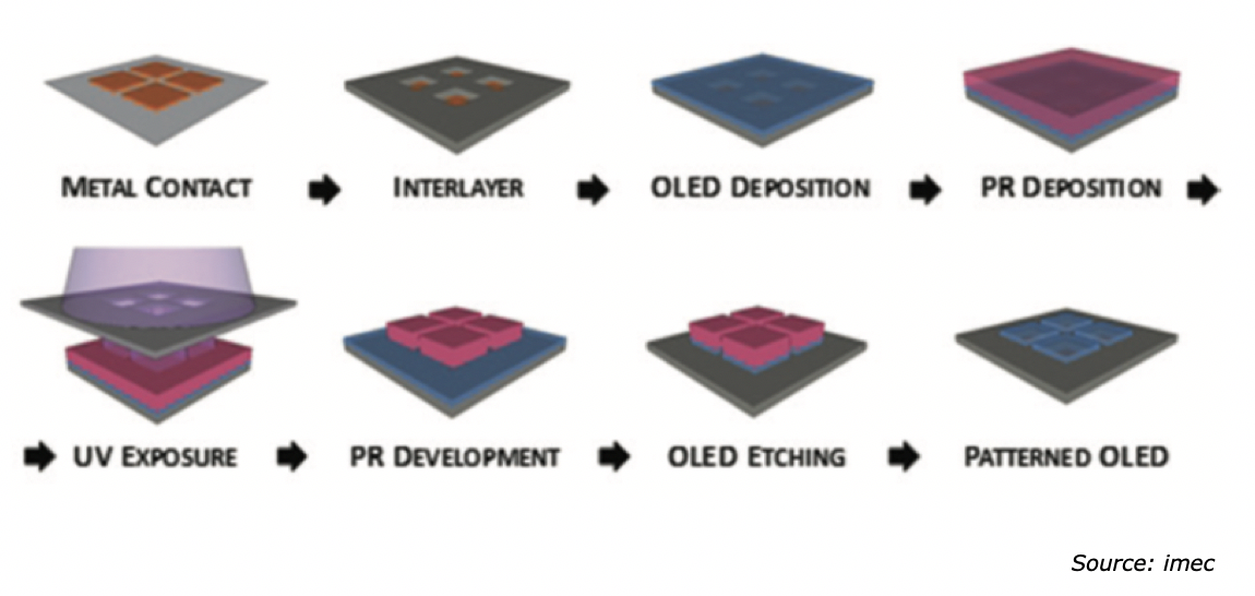
Side-by-side RGB pixels using photolithography starts after an OLED stack, photoresist is used to transfer the pattern and remove the unnecessary material by etching. The challenge is the susceptibility of OLED materials to solvents – using standard (semiconductor) photoresist chemistry results in dissolution/removal of the stack. Still, the gains in pixel density may be worth the effort, as lithography enables submicron pixel pitch and very high aperture ratio (emitting area maximized thanks to minimizing pixel spacing). Over the years, other approaches for photolithography have been proposed. Orthogonal Inc, uses fluorinated materials which should not have any chemical interaction with the organic stacks (thus, orthogonal to OLED). The other approach, followed by imec together with Fujifilm, is to pattern organic stacks using a non-fluorinated, chemically amplified photoresist system.
Figure 1: Photolithography Steps to Pattern the Light Emitting Layer
AR and VR applications have very aggressive requirements in terms of pixel density in order to avoid annoying “pixilation.” The same goes for required minimum pixel spacing, to avoid “screen door effect”. With photolithography, these two challenges can be addressed simultaneously. The OSR photoresist system from Fujifilm can deliver lines and spaces with 1 μm pitch, which fits in the roadmap towards several thousand ppi resolution for the OLED front plane.
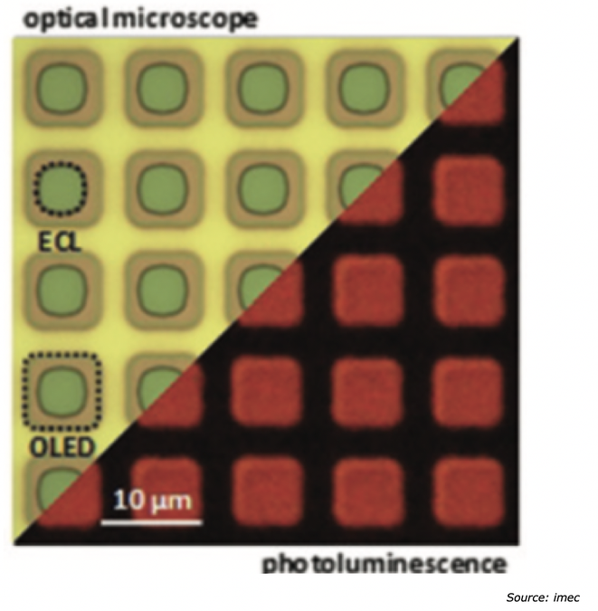
Figure 2: Example Of 3 mm Pitch Panel
Figure 2: Example Of 3 mm Pitch Panel
Another limitation is the resolution of the PDL (pixel definition layer), a dielectric layer separating the OLED stack from the bottom contact level. The resolution of this layer limits the maximum opening that can be achieved, which translates to the aperture ratio of the pixel – or the percentage of the area that is used for OLED emission. In this example, the “photoluminescence aperture ratio”, or the relation of the OLED island to the pixel area is around 50%, which is enabled by small spacing (<3 μm). However, the “electroluminescence aperture ratio”, of the relation of the area emitting light, is 25% because of the PDL area and the necessary overlap of the OLED island. Assuming minimum line spacing of 1 μm, results in a PL ratio of 81% (9 x 9 μm) and EL ratio of 64% (8 x 8 μm) for a subpixel of 10 x 10 μm. With such scaling, the usable area of the array can be enlarged, which results in longer device lifetime (since we can reduce the driving current density) and in reduction or elimination of the screen-door effects.
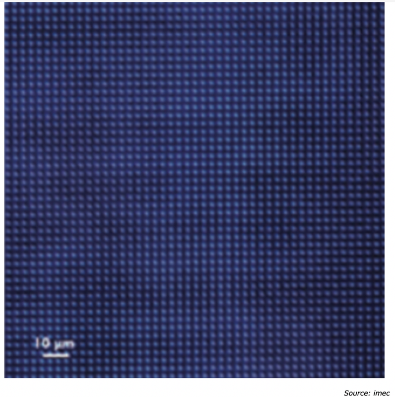
Figure 3: Monochrome OLED Array w/10 μm pitch
Figure 3: Monochrome OLED Array w/10 μm pitch
Obviously, interrupting the optimum deposition process in ultra-high vacuum and exposing the OLED stack to photolithography materials has an impact on the device performance. Just breaking the vacuum results in a lifetime performance hit. Additionally, the initial process flow includes exposure of the stack to ambient atmosphere (air and humidity), using standard cleanroom equipment. In the beginning, such “worst case scenario” resulted in proof-of-concept of emitting OLEDs after patterning, but, unsurprisingly, with device lifetime of only few minutes. In the course of the development, imec improved on three fronts.
- Firstly, there have been continuous upgrades of the photoresist system to make it more compatible with the organic stack.
- Secondly, the process flow has been optimized to reduce the impact of process parameters on device performance.
- Thirdly, the OLED stacks have been tuned for robustness, for example by introducing additional protection layers for the most critical interfaces. All these actions resulted in device lifetimes of several hundred hours at 1000 nit luminance. As the lifetime is the major concern when it comes to the readiness of this technology, this is an ongoing effort to bring all the parameters to a level acceptable by the industry.
|
Contact Us
|
Barry Young
|


