Focus on the 6th Annual China OLED Summit
January 23, 2017 Kazuhiro Noda, JOLED R&D Division Manage, spoke at he conference. JOLED was formed by taking OLED staff and equipment from Panasonic and Sony and funding from INCJ and JDI. The resulting ownership was
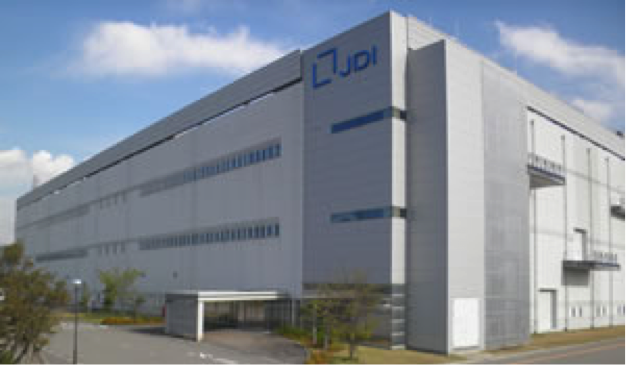
Recently, JDI added US$100m in capital and now holds a larger ownership position. JOLED was formed to develop OLED displays for the “middle market”, which they define are monitors, notebooks and tablets that are 10”-15” in diagonal. The technology that will be used is R G B printing (using polymer material from Sumitomo, a one-off ink jet printer from Panasonic and TAOS, which is amorphous oxide backplane from Sony. They are also pursuing plastic substrates. Noda showed Figure 1 JDI’s Ishikawa Fab Source: JDI the following chart, which showed that they have reduced power consumption on 1 12.2” FHD equivalent operating at 350 cd/m2 by 98% beginning in 2008. However, Noda did not say what the original or current power consumption was. From a backplane perspective, they have tried ES-type Bottom gate, CE Type Bottom Gate and have now landed on Self-Aligned Top Gate; dropping from 8 masks to 5 masks. JOLED is currently, operating a Gen 4.5 pilot line, where they produce 10” to 30” panels. Their schedule is to continue product verification thru 2020, while building a production line in 2018/19 and then start mass production in the middle of 2019. Clearly, this begs the issue of why go after the IT market, where white is so prevalent causing relatively high power consumption. When asked about moving to TVs, Noda simple answered buy saying this was the corporate direction. Figure 2 Power Consumption Improvements
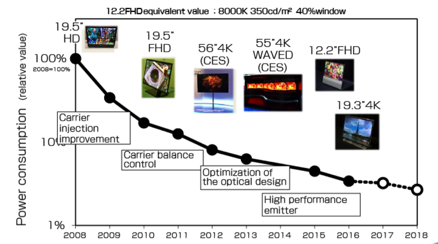
Source: JDI
|
Vertical Divider
|
Search by typing & pressing enter