Vertical Divider
Active-Matrix OLED Displays Attached to Human Skin
July 26, 2020
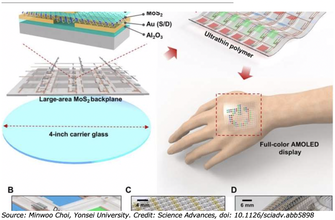
In a new report on Science Advances, Minwoo Choi and a team of scientists in Electronic Engineering and Materials Science in the Republic of Korea, developed a wearable, full-color OLED display using a two-dimensional (2-D) material-based backplane transistor. They engineered an 18-by-18 thin-film transistor array on a thin molybdenum disulfide (MoS2) film and transferred it to an aluminum oxide(Al2O3)/polyethylene terephthalate (PET) surface. Choi et al. then deposited red, green and blue OLED pixels on the device surface and observed excellent mechanical and electrical properties of the 2-D material. The surface could drive circuits to control the OLED pixels to form an ultrathin, wearable device. The following figure shows the full-color AMOLED display with large-area MoS2-based backplane. (A) Schematic illustration of the high-performance MoS2-based backplane on a 4-inch carrier glass substrate, where an Al2O3 capping layer was applied for n-doping effects on the MoS2 film (top left), an active-matrix full-color display was applied to the ultrathin polymer substrate (top right), and the large-area full-color display was tested on a human hand (bottom right).
Figure 1: Components of a Wearable, Full-Color OLED Display
(B) Scheme of the active-matrix full-color pixel array integrated with MoS2 transistors, where each pixel was connected via a gate, data, and cathode interconnector for line-addressing control. (C) Digital photograph of the active-matrix display on the 4-inch carrier glass substrate, where the inset demonstrates the full-color display when switched on. (D) Digital photograph of the large-area full-color display on the ultrathin polymer substrate, demonstrating the flexible mechanical properties due to the low bending stiffness of the ultrathin material.
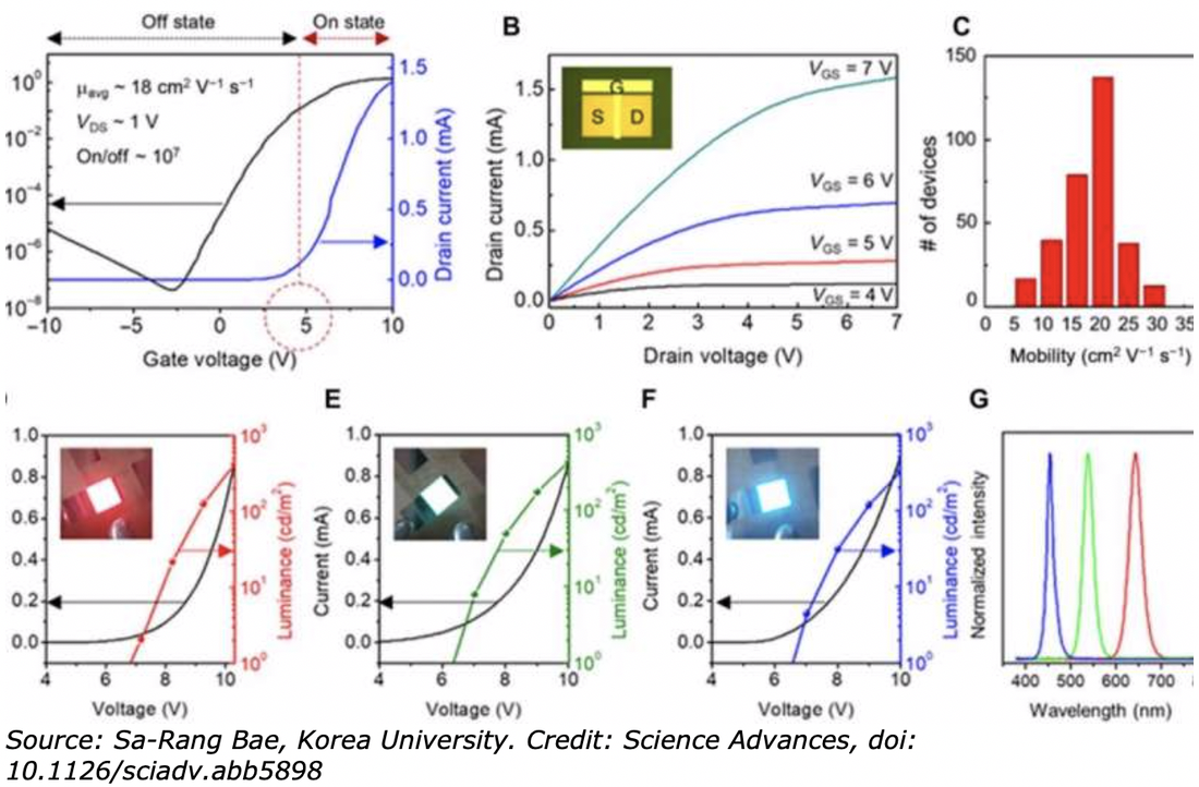
The requirements for a thin, stable device pushed the researchers to use alternative semiconductor materials such as MoS2, which has relatively high performance thin-film transistors (TFTs) and logic circuits. These materials called transition metal dichalcogenides provide unique electrical, optical, and mechanical properties for backplane circuitry of wearable electronics. Researchers developed MoS2 transistors with the red, green and blue (RGB) colors needed for displays. Choi et al. developed a large-area MoS2 TFT array to operate 324 pixels in a 2-inch RGB OLED. The RGB OLEDs were made of different optoelectronic characteristics, therefore the team designed the backplane TFTs to control each color pixel separately. The wearable display was attached to human skin without adverse effects. The team used heterogenous material designs to form optoelectronics in the present work. The next figure shows the (A) Transfer curve of the MoS2 transistor on the 4-inch carrier glass substrate, where the average mobility of 18 cm2 V−1 s−1 was sufficient for operating the RGB OLEDs. (B) I-V characteristics of the MoS2 transistor as the gate bias was increased from +4 to 7 V, where the inset shows the MoS2 transistor. (C) Statistical analysis of the MoS2 transistor mobility across 324 samples. (D to F) I-V characteristics (left y axis) and luminance (right y axis) of the RGB OLED as a function of applied bias, where the insets visualize the emission of each OLED color. (G) EL spectra of the RGB OLED pixels.
Figure 2: Device Properties Of The Mos2 Transistor And RGB OLEDs
A large-area active-matrix OLED display with an MoS2 backplane was also designed by:
The full-color AMOLED display uniformly controlled the RGB OLED pixels, where similar to typical displays, each pixel was connected to a data and a scanning line. Choi et al. controlled the pixel current based on the drain and gate signals of the transistor to change the brightness of the OLED. They could then transfer the ultrathin display from the carrier glass substrate to a curved surface without device degradation.
Figure 3: Dynamic Operation Of The Active-Matrix Display Using External Circuit Control
- Forming a TFT array on a thin MoS2 film, by synthesizing a bilayer MoS2 film on a 4-inch SiO2/Si wafer via metal organic chemical vapor deposition (MOCVD).
- Coated a polyethylene terephthalate (PET) substrate with aluminum oxide using atomic layer deposition and transferred the MoS2 film from the SiO2/Si wafer to the PET substrate to produce an MoS2 transistor array with a driving backplane configuration.
- Depositing RGB OLEDs on the drain electrode of the TFTs
- Peeling the display from the carrier to transfer it to the human hand (the target).
- Encapsulating the device with aluminum oxide for improved metal contacts and carrier mobility.
The full-color AMOLED display uniformly controlled the RGB OLED pixels, where similar to typical displays, each pixel was connected to a data and a scanning line. Choi et al. controlled the pixel current based on the drain and gate signals of the transistor to change the brightness of the OLED. They could then transfer the ultrathin display from the carrier glass substrate to a curved surface without device degradation.
Figure 3: Dynamic Operation Of The Active-Matrix Display Using External Circuit Control
The homogeneity of the MOCVD-grown MoS2 film allowed high uniformity for stable display applications. The device properties were consistent across all the samples, allowing a single pixel to operate in the full-color AMOLED, while the efficiency did not decrease. At the highest luminescence the color wavelengths were 460, 530, and 650 nm for blue, green and red. Using a repeated gate pulse bias of +10 volts, the OLED exhibited a rapid transition between on and off states, although the response time measurements were limited by the system, the delay time was short. Gate modulation did not occur during the off state and the pixel state remained stable, providing efficient leak-proof operation of the TFT. The pixel current also dramatically increased with increasing gate bias (VG) during the on state to reach a threshold voltage of 5 volts across the RGB OLEDs.
Figure 4: The Properties Of A Single Pixel Integrated With The Mos2 Transistor And RGB OLEDs.
(A) Schematic illustration of the RGB unit pixels integrated with the MoS2 transistor in a series connection for active-matrix configuration. (B) Pixel-switching properties controlled using a gate bias of −10 and 10 V at fixed data biases of 4 V (red) and 10 V (blue). (C) Digital photograph of the luminance change in the RGB OLEDs in a gate bias range of 4 to 9 V, where the brightness of each OLED was stable and controlled by the gate signal of the MoS2 transistor. (D to F) The pixel current (left y axis) and luminance (right y axis) as a function of gate signal.
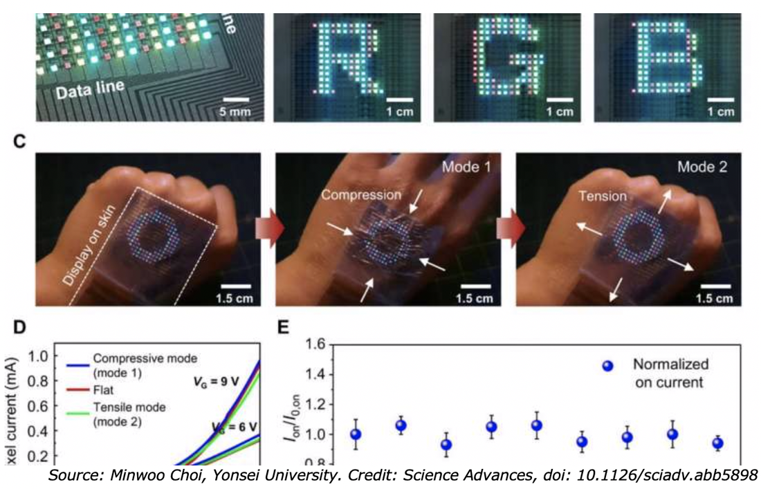
The subpixel performance was confirmed using an 18 x 18 array (324 pixels) device. Each subpixel was controlled via the matrix line and maintained consistent light luminescence. The RGB OLED pixels showed consistent and uniform brightness due to the stable control of the gate and data signals. Choi et al. drove the RGB pixel arrays sequentially via an external drive circuit configured in a commercial strip pixel structure representing the characters 'R', 'G', and 'B'. The low stiffness of the ultrathin device prevented the deterioration of optical and electrical properties during substantial mechanical deformation reflexes—after its transfer to a human hand. Based on the I-V characteristics, the current level was uniform during skin shrinkage or skin stretching exercises and the on-state did not fluctuate during operation. While the device stability is still in development, the team expects to improve the MoS2 film for a wearable, full-color AMOLED display.
Figure 5: Digital Photographs Of The Full-Color Active-Matrix Display
(A) the “all on” state; (B) the dynamic operation of the active-matrix display, where gate and data signals were individually controlled using the external circuit; and (C) the application of the ultrathin display on a human hand, where the display was deformed by two mechanical modes based on hand motion, namely, compressive mode (center) and tensile mode (right). (D) Plots of the unit pixel current as a function of data voltage at VG values of 4 V (off state), 6 V, and 9 V in the compressive (blue), flat (red), and tensile (green) mode. At every applied gate bias (VG), negligible change in pixel current is observed under various modes of deformation, which enables stable operation of AMOLED on human hand. (E) Normalized on-state current variation of the ultrathin display on human hand during mechanical deformation.
In summary, Choi and colleagues developed a thin (2-inch), wearable and full-color AMOLED display with 18 x 18 arrays using MoS2-based backplane TFTs, built on a bilayer MoS2 film grown using MOCVD and observed high carrier mobility and on/off ratios. They controlled the light emission by applying a gate-voltage between 4 and 9 volts. They used an ultrathin plastic substrate (PET) combined with 2-D semiconducting materials to fabricate display with high electrical, optical, and mechanical performance. This experimental system can be improved for integration in wearable and electronic devices beyond the existing conventional and rigid organic materials. From: Thamarasee Jeewandara , Phys.org
|
Contact Us
|
Barry Young
|


