Vertical Divider
|
Silicon Wafers—The µLEDs Building Block
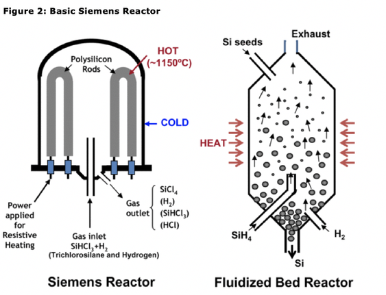
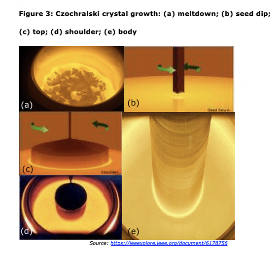
Silicon wafers are grown from metallurgical grade polysilicon, which is produced by mixing silica (Silicon Dioxide – SiO2) with Carbon and heating to 1,900⁰C in an arc furnace and is then converted to TCS (Trichlorosilane – SiHCl3), a liquid and further refined through distillation. The TCS is then converted to solid polysilicon through the Siemens process, and then reheated in a crucible (Czochralski Method). A seed crystal is dipped into the melt and is slowly pulled from the liquid as the silicon grows around the seed. By controlling the heat and ‘pull’ rate, the size of the silicon rod can be set. About 80% of the world's polysilicon is produced using the Siemen's process developed in the 1950s. (a) Basic Siemen's reactor. (b) As grown polysilicon rods after a reactor run. (Current generation reactors have many more rods.) (c) Final polysilicon chunks ready for loading into a crystal growth furnace. 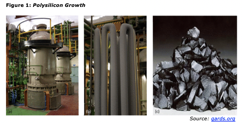
|
|