Vertical Divider
100nm Thick Sapphire Nano-Membrane Array Used to Grow Discrete 4 μm MicroLEDs
Researchers from Seoul National University, KAIST, Korea Photonics Institute and SAIT are developing a new method to deposit microLEDs on sapphire nano-membranes, which enables chip singulation without the need for an etching process to produce microLED devices. MicroLED display manufacturing is faced with low external quantum efficiency (EQE), high leakage current and an expensive transfer process.
Researchers from Seoul National University, KAIST, Korea Photonics Institute and SAIT are developing a new method to deposit microLEDs on sapphire nano-membranes, which enables chip singulation without the need for an etching process to produce microLED devices. MicroLED display manufacturing is faced with low external quantum efficiency (EQE), high leakage current and an expensive transfer process.
- Low EQEs and high leakage current have been attributed to plasma etching - a step that is commonly used during device fabrication as part of the chip singulation process. The extent of these problems increases inversely to the size of the chip
- The lattice mismatch and the difference in thermal expansion coefficients between the LEDs (typically GaN-based) induces high defect densities and high compressive stress in GaN layers which, in turn, degrade LED performance.
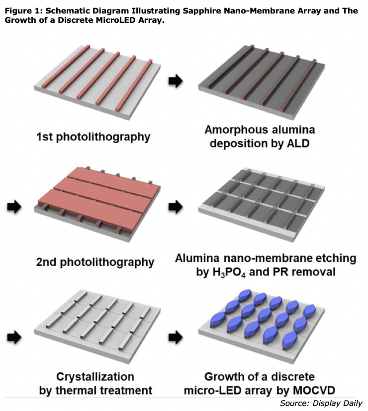
The sequence used in the fabrication of a sapphire nano-membrane array and the subsequent growth of a discrete microLED array is shown in the figure below. “The sapphire nano-membrane array was fabricated photolithography, atomic layer deposition (ALD) of amorphous alumina, alumina nano-membrane etching for the formation of an array by phosphoric acid (H3PO4) and subsequent crystallization by thermal treatment. During the thermal annealing, the amorphous alumina nano-membrane array was crystallized into single crystalline sapphire (α-phase) by solid phase epitaxy. Then, a microLED array could be separately grown on a sapphire nano-membrane array without the need for a chip singulation process.”
A few top level results include the following:
Researchers at the Guangdong Institute of Semiconductor Industrial Technology (GISIT), the University of Tokyo, and Foshan Debao Display Technology Co Ltd have recently developed a tape-assisted laser lift-off transfer (TALT) technique, addressing the industry’s problems of massive chip transfer and heterogeneous integration of micro-LED for high-resolution display purposes [Zhangxu Pan et al, ‘Wafer-Scale Micro-LEDs Transferred onto an Adhesive Film for Planar and Flexible Displays’, Advanced Material Technology, https://doi.org/10.1002/admt.202000549].
Recognized as a next-generation display technology in the display industry, micro-LEDs have many advantages such as higher brightness, lower power consumption, longer lifetime, higher resolution and faster response speed compared with conventional liquid crystal display (LCD) and organic light-emitting diode (OLED) display technologies. They are therefore expected to have very good application prospects in wearable electronic devices, outdoor displays and augmented reality/virtual reality (AR/VR) head-mounted displays.
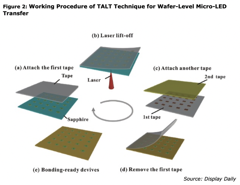
However, the volume production of high-resolution micro-LED display devices currently faces many challenges. Among them, how to quickly and accurately transfer and integrate millions of micro-LED chips onto the drive circuit is a major hurdle to be overcome. Although a variety of transfer technologies for micro-LEDs have been proposed, there is still ample room for improvement in their transfer speed and placement accuracy. In addition, most of these transfer technologies are focused on the optimization of the chip transfer technology itself, but less attention is paid to their compatibility with subsequent bonding processes. The joint teams have exploited the merits of both laser lift-off and tape transfer to fabricate wafer-level thin-film micro-LEDs. The novel TALT technique for fabricating thin-film micro-LEDs transferred to a temporary adhesive substrate is shown in next figure. An adhesive tape is laminated onto the micro-LED arrays on a sapphire substrate [next figure (a)]. The sapphire substrate is then taken off by laser lift-off (LLO). As a result, wafer-scale micro-LED arrays are then released to the first adhesive tape [Figure 1 (b)]. Before flip-chip bonding to a driver board, micro-LEDs must be turned upside down. This is achieved by attaching another tape with stronger adhesion to the full LED arrays on the first tape [next figure (c)]. Because of the stronger adhesion, micro-LEDs can be released to the second tape. This is achieved by simply peeling away the first tape [next figure (d)]. Now, transferrable thin-film micro-LEDs, which are particularly suited to flip-chip bonding, are ready [next figure (e)].
A few top level results include the following:
- The strain in GaN associated with the lattice mismatch between GaN and sapphire substrate was shared with the ultra-thin sapphire nano-membrane. As a consequence, threading dislocation density in the microLEDs was reduced by 59.6% compared to GaN formed on a conventional planar substrate.
- The method improved the internal quantum efficiency of the microLEDs by 44% compared to conventional GaN microLEDs produced on regular planar substrates.
- The microLEDs provided 3.3 times the photoluminescence compared to conventional microLEDs.
- The nano-membranes could be broken using mechanical force. By this means, the microLEDs could be easily separated from the substrate and transferred to the final backplane – without the need for potentially harmful plasma etching.
Researchers at the Guangdong Institute of Semiconductor Industrial Technology (GISIT), the University of Tokyo, and Foshan Debao Display Technology Co Ltd have recently developed a tape-assisted laser lift-off transfer (TALT) technique, addressing the industry’s problems of massive chip transfer and heterogeneous integration of micro-LED for high-resolution display purposes [Zhangxu Pan et al, ‘Wafer-Scale Micro-LEDs Transferred onto an Adhesive Film for Planar and Flexible Displays’, Advanced Material Technology, https://doi.org/10.1002/admt.202000549].
Recognized as a next-generation display technology in the display industry, micro-LEDs have many advantages such as higher brightness, lower power consumption, longer lifetime, higher resolution and faster response speed compared with conventional liquid crystal display (LCD) and organic light-emitting diode (OLED) display technologies. They are therefore expected to have very good application prospects in wearable electronic devices, outdoor displays and augmented reality/virtual reality (AR/VR) head-mounted displays.
However, the volume production of high-resolution micro-LED display devices currently faces many challenges. Among them, how to quickly and accurately transfer and integrate millions of micro-LED chips onto the drive circuit is a major hurdle to be overcome. Although a variety of transfer technologies for micro-LEDs have been proposed, there is still ample room for improvement in their transfer speed and placement accuracy. In addition, most of these transfer technologies are focused on the optimization of the chip transfer technology itself, but less attention is paid to their compatibility with subsequent bonding processes. The joint teams have exploited the merits of both laser lift-off and tape transfer to fabricate wafer-level thin-film micro-LEDs. The novel TALT technique for fabricating thin-film micro-LEDs transferred to a temporary adhesive substrate is shown in next figure. An adhesive tape is laminated onto the micro-LED arrays on a sapphire substrate [next figure (a)]. The sapphire substrate is then taken off by laser lift-off (LLO). As a result, wafer-scale micro-LED arrays are then released to the first adhesive tape [Figure 1 (b)]. Before flip-chip bonding to a driver board, micro-LEDs must be turned upside down. This is achieved by attaching another tape with stronger adhesion to the full LED arrays on the first tape [next figure (c)]. Because of the stronger adhesion, micro-LEDs can be released to the second tape. This is achieved by simply peeling away the first tape [next figure (d)]. Now, transferrable thin-film micro-LEDs, which are particularly suited to flip-chip bonding, are ready [next figure (e)].
The resulting wafer-level micro-LED thin film is shown in the next figure. The results in next figure (a) and (b) clearly show that a very high yield of micro-LED lift off (up to 99.9%) can be achieved under optimized LLO conditions. Both the optical and electrical tests suggest that the device before transfer and after transfer shows minimal degraded device performance [next figure s 2(c) and (d)]. The researchers believe that this method has the potential for wafer-scale production, and can even be scaled up to larger-size wafers.
The researchers emphasized that the TALT technology is suitable not only for wafer-level transfer of micro-LEDs but also for flip-chip bonding for good electrical connection. Indeed, the researchers have further demonstrated both rigid and flexible micro-LED prototypes with convincing device performances, based on the TALT technique and the bump-less bonding process that the same joint team has developed. Representative flexible micro-LED devices are shown in the next figure.
The researchers said the technique paves the way for fast assembly of micro-LEDs with high yield and excellent placement accuracy. The method is also promising for fabricating high-resolution micro-display devices for potential applications in areas such as VR/AR headsets, wearables and mini-projectors. Source: Display Daily
|
Contact Us
|
Barry Young
|


